SLVSD38C November 2015 – August 2021 TPS61089
PRODMIX
- 1 Features
- 2 Applications
- 3 Description
- 4 Revision History
- 5 Device Comparison Table
- 6 Pin Configuration and Functions
- 7 Specifications
- 8 Detailed Description
- 9 Application and Implementation
- 10Power Supply Recommendations
- 11Layout
- 12Device and Documentation Support
- 13Mechanical, Packaging, and Orderable Information
Package Options
Mechanical Data (Package|Pins)
- RNR|11
Thermal pad, mechanical data (Package|Pins)
Orderable Information
9.2.2.8 Loop Stability
The TPS61089x requires external compensation, which allows the loop response to be optimized for each application. The COMP pin is the output of the internal error amplifier. An external compensation network comprised of resistor R5, ceramic capacitors C5 and C6 is connected to the COMP pin.
The power stage small signal loop response of constant off time (COT) with peak current control can be modeled by Equation 11.
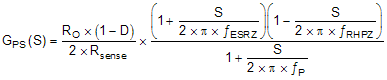
where
- D is the switching duty cycle
- RO is the output load resistance
- Rsense is the equivalent internal current sense resistor, which is 0.08 Ω
- ƒP is the pole's frequency
- ƒESRZ is the zero's frequency
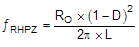
- ƒRHPZ is the right-half-plane-zero's frequency
The D, ƒP, ƒESRZ, and ƒRHPZ can be calculated by following equations:

where
- η is the power conversion efficiency
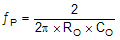
where
- CO is effective capacitance of the output capacitor
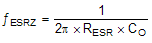
where
- RESR is the equivalent series resistance of the output capacitor
The COMP pin is the output of the internal transconductance amplifier. Equation 16 shows the small signal transfer function of compensation network.
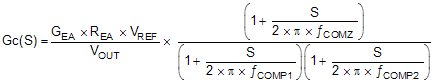
where
- GEA is the amplifier’s transconductance
- REA is the amplifier’s output resistance
- VREF is the refernce voltage at the FB pin
- VOUT is the output voltage
- ƒCOMP1, ƒCOMP2 are the poles' frequency of the compensation network
- ƒCOMZ is the zero's frequency of the compensation network
The next step is to choose the loop crossover frequency, ƒC. The higher in frequency that the loop gain stays above zero before crossing over, the faster the loop response is. It is generally accepted that the loop gain cross over no higher than the lower of either 1/10 of the switching frequency, ƒSW, or 1/5 of the RHPZ frequency, ƒRHPZ.
At the crossover frequency, the loop gain is 1. Thus the value of R5 can be calculated by Equation 17, then set the values of C5 and C6 (in Figure 9-1) by Equation 18 and Equation 19.
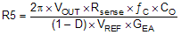
where
- ƒC is the selected crossover frequency
The value of C5 can be set by Equation 18.

The value of C6 can be set by Equation 19.
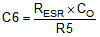
If the calculated value of C6 is less than 10 pF, it can be left open.
Designing the loop for greater than 45° of phase margin and greater than 10-dB gain margin eliminates output votlage ringing during the line and load transient.