SLVSD38C November 2015 – August 2021 TPS61089
PRODMIX
- 1 Features
- 2 Applications
- 3 Description
- 4 Revision History
- 5 Device Comparison Table
- 6 Pin Configuration and Functions
- 7 Specifications
- 8 Detailed Description
- 9 Application and Implementation
- 10Power Supply Recommendations
- 11Layout
- 12Device and Documentation Support
- 13Mechanical, Packaging, and Orderable Information
Package Options
Mechanical Data (Package|Pins)
- RNR|11
Thermal pad, mechanical data (Package|Pins)
Orderable Information
9.2.2.5 Inductor Selection
Because the selection of the inductor affects the steady state operation of the power supply, transient behavior, loop stability, and boost converter efficiency, the inductor is the most important component in switching power regulator design. Three most important specifications to the performance of the inductor are the inductor value, DC resistance, and saturation current.
The TPS61089x is designed to work with inductor values between 0.47 µH and 10 µH. A 0.47-µH inductor is typically available in a smaller or lower-profile package, while a 10-µH inductor produces lower inductor current ripple. If the boost output current is limited by the peak current protection of the IC, using a 10-µH inductor can maximize the controller’s output current capability.
Inductor values can have ±20% or even ±30% tolerance with no current bias. When the inductor current approaches saturation level, its inductance can decrease 20% to 35% from the value at 0-A current depending on how the inductor vendor defines saturation. When selecting an inductor, make sure its rated current, especially the saturation current, is larger than its peak current during the operation.
Follow Equation 6 to Equation 7 to calculate the peak current of the inductor. To calculate the current in the worst case, use the minimum input voltage, maximum output voltage, and maximum load current of the application. To leave enough design margin, TI recommends using the minimum switching frequency, the inductor value with –30% tolerance, and a low-power conversion efficiency for the calculation.
In a boost regulator, calculate the inductor DC current as in Equation 6.
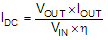
where
- VOUT is the output voltage of the boost regulator
- IOUT is the output current of the boost regulator
- VIN is the input voltage of the boost regulator
- η is the power conversion efficiency
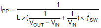
Calculate the inductor current peak-to-peak ripple as in Equation 7.
where
- IPP is the inductor peak-to-peak ripple
- L is the inductor value
- ƒSW is the switching frequency
- VOUT is the output voltage
- VIN is the input voltage
Therefore, the peak current, ILpeak, seen by the inductor is calculated with Equation 8.
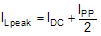
Set the current limit of the TPS61089x higher than the peak current ILpeak. Then select the inductor with saturation current higher than the setting current limit.
Boost converter efficiency is dependent on the resistance of its current path, the switching loss associated with the switching MOSFETs, and the core loss of the inductor. The TPS61089x has optimized the internal switch resistance. However, the overall efficiency is affected significantly by the DC resistance (DCR) of the inductor, equivalent series resistance (ESR) at the switching frequency, and the core loss. Core loss is related to the core material and different inductors have different core loss. For a certain inductor, larger current ripple generates higher DCR and ESR conduction losses and higher core loss. Usually, a data sheet of an inductor does not provide the ESR and core loss information. If needed, consult the inductor vendor for detailed information. Generally, TI would recommend an inductor with lower DCR and ESR. However, there is a tradeoff among the inductance of the inductor, DCR and ESR resistance, and its footprint. Furthermore, shielded inductors typically have higher DCR than unshielded inductors. Table 9-2 lists recommended inductors for the TPS61089x. Verify whether the recommended inductor can support the user's target application with the previous calculations and bench evaluation. In this application, the Sumida inductor CDMC8D28NP-1R8MC is selected for its small size and low DCR.
| PART NUMBER | L (µH) | DCR MAX (mΩ) | SATURATION CURRENT / HEAT RATING CURRENT (A) | SIZE MAX (L × W × H mm) |
VENDOR |
|---|---|---|---|---|---|
| CDMC8D28NP-1R8MC | 1.8 | 12.6 | 9.4 / 9.3 | 9.5 x 8.7 x 3.0 | Sumida |
| 744311150 | 1.5 | 7.2 | 14.0 / 11.0 | 7.3 x 7.2 x 4.0 | Wurth-Elektronik |
| 744311220 | 2.2 | 12.5 | 13.0 / 9.0 | 7.3 × 7.2 × 4.0 | Wurth-Elektronik |
| PIMB103T-2R2MS | 2.2 | 9.0 | 16 / 13 | 11.2 × 10.3 × 3.0 | Cyntec |
| PIMB065T-2R2MS | 2.2 | 12.5 | 12 / 10.5 | 7.4 × 6.8 × 5.0 | Cyntec |