SLVS625E February 2006 – November 2015 TPS61150 , TPS61151
PRODUCTION DATA.
- 1 Features
- 2 Applications
- 3 Description
- 4 Revision History
- 5 Device Comparison Tables
- 6 Pin Configuration and Functions
- 7 Specifications
- 8 Detailed Description
- 9 Application and Implementation
- 10Power Supply Recommendations
- 11Layout
- 12Device and Documentation Support
- 13Mechanical, Packaging, and Orderable Information
Package Options
Mechanical Data (Package|Pins)
- DRC|10
Thermal pad, mechanical data (Package|Pins)
- DRC|10
Orderable Information
9 Application and Implementation
NOTE
Information in the following applications sections is not part of the TI component specification, and TI does not warrant its accuracy or completeness. TI’s customers are responsible for determining suitability of components for their purposes. Customers should validate and test their design implementation to confirm system functionality.
9.1 Application Information
The standard application circuit is shown in Figure 8. Typical VIN range is from a single cell Li+ battery. LED strings voltages can be as high as 28 V (TPS61150) or 22 V (TPS61151). LED string voltage mismatch is allowed due to the adaptive feedback headroom voltage which dynamically looks for and regulates the highest voltage string.
9.2 Typical Application
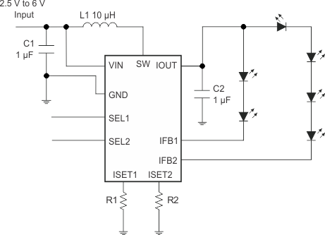 Figure 8. TPS6115x Typical Application
9.2.1 Design Requirements
For typical dual output boost WLED driver applications, use the parameters listed in Table 4.
Table 4. Design Parameters
| DESIGN PARAMETER | EXAMPLE VALUE |
|---|---|
| Minimum input voltage | 2.5 V |
| Minimum output voltage | VIN |
| Output current | up to 35 mA/string |
| Fixed switching frequency | 1.2 MHz |
9.2.2 Detailed Design Procedure
9.2.2.1 Maximum Output Current
The overcurrent limit in a boost converter limits the maximum input current (and thus the maximum input power) for a given input voltage. Maximum output power is less than the maximum input power because of power conversion losses. Therefore, the current limit, input voltage, output voltage, and efficiency can all change maximum current output. Because current limit clamps peak inductor current, ripple must be subtracted to derive the maximum DC current. The ripple current is a function of switching frequency, inductor value, and duty cycle. Equation 2 and Equation 3 take all of the above factors into account for maximum output current calculation.

where
- IP = inductor peak to peak ripple
- L = inductor value
- VF = power diode forward voltage
- FS = switching frequency
- VIOUT = boost output voltage. It is equal to 330 mV + voltage drop across WLED.

where
- IOUT_MAX = maximum output current of the boost converter
- ILIM = overcurrent limit
- η = efficiency
To keep a tight range on the overcurrent limit, the TPS6115x uses the VIN and IOUT pin voltages to compensate for the overcurrent limit variation caused by the slope compensation. However, the current threshold still has a residual dependency on the VIN and IOUT voltages. Use Figure 1 and Figure 2 to identify the typical overcurrent limit in a specific application, and use a ±25% tolerance to account for temperature dependency and process variations.
The maximum output current can also be limited by the current capability of the current-sink circuitry. It is designed to provide a maximum 35-mA current regardless of the current capability of the boost converter.
9.2.2.2 WLED Brightness Dimming
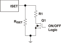
There are three ways to change the output current on the fly for WLED dimming. The first method parallels an additional resistor with the ISET pin resistor as shown in Figure 9. The switch (Q1) can change the ISET pin resistance, and therefore modify the output current. This method is very simple, but can provide only limited dimming steps.
Alternatively, a PWM dimming signal at the SEL pin can modulate the output current by the duty cycle of the signal. The logic high of the signal turns on the current sink circuit, while the logic low turns it off. This operation creates an averaged DC output current proportional to the duty cycle of the PWM signal. The frequency of the PWM signal must be high enough to avoid flashing of the WLEDs. The soft start of the current sink circuit is disabled during the PWM dimming to improve linearity.
The major concern of the PWM dimming is the creation of audible noises that can come from the inductor or output capacitor of the boost converter, or both. The audible noises on the output capacitor are created by the presence of voltage ripple in range of audible frequencies. The TPS6115x alleviates the problem by disconnecting the WLEDs from the output capacitor when the SEL pin is low. Therefore, the output capacitor is not discharged by the WLEDs, and thus reduces the voltage ripple during PWM dimming.
The audible noises can be eliminated by using a PWM dimming frequency above or below the audible frequency range. The maximum PWM dimming frequency of the TPS6115x is determined by the current settling time (Tisink), which is the time required for the sink circuit to reach a steady state after the SEL pin transitions from low to high. The maximum dimming frequency can be calculated by Equation 4:

where
- DMIN = min duty cycle of the PWM dimming required in the application
For 20% DMIN, a PWM dimming frequency up to 33 kHz is possible, putting the noise frequency above the audible range.
Because the TPS61150/1 dynamically regulates one IFB pin voltage, its output voltage can have a large ripple during PWM dimming as shown in Figure 6. This ripple may cause ceramic output capacitors to ring audibly. To reduce the output ripple, the configurations shown in Figure 16 and Figure 17 are recommended for PWM dimming. In Figure 16, both current strings have the same number of LEDs and the same PWM signal. In Figure 17, one string (in this case, string 2) is not PWM dimmed and has a greater total forward voltage drop than string 1, either because of having more LEDs than string 1 or because of adding a resistor in series with string 2. Therefore, IFB2 controls the regulation regardless of the PWM signal on IFB1, and the output ripple is significantly reduced when string 1 is dimmed. The circuit in Figure 17 could have been reconfigured with string 1 having the larger total forward drop.
The third method uses an external DC voltage and resistor as shown in Figure 10 to change the ISET pin current, and thus control the output current. The DC voltage can be the output of a filtered PWM signal. The formulas to calculate the output current is given by Equation 5 and Equation 6.


where
- KISET = current multiplier between the ISET pin current and the IFB pin current.
- VDC= voltage of the DC voltage source or the DC voltage of the PWM signal.
 Figure 10. Analog Dimming Using an External Voltage Source to Control the Output Current
9.2.2.3 Inductor Selection
Because the selection of the inductor affects the power supply steady-state operation, transient behavior, and loop stability, the inductor is the key component in power regulator design. Three specifications are the most important to the performance of the inductor: the inductor value, DC resistance (DCR), and saturation current. Considering the inductor value alone is not enough.
The inductor inductance value determines the inductor ripple current. It is generally recommended to set peak-to-peak ripple current given by Equation 2 to betweeen 30% to 40% of DC current. It is a good compromise of power loss and inductor size. For this reason, 10-μH inductors are recommended for the TPS6115x. Inductor DC current can be calculated as Equation 7.

Use the maximum load current and minimum Vin for calculation.
The internal loop compensation for PWM control is optimized for the external component shown in the Figure 8 with consideration of component tolerance. Inductor values can have ±20% tolerance with no current bias. When the inductor current approaches saturation level, its inductance can decrease 20% to 35% from the 0-A value, depending on how the inductor vendor defines saturation. Using an inductor with a smaller inductance value forces discontinuous PWM in which the inductor current ramps down to zero before the end of each switching cycle, reduces the boost converter maximum output current, and causes large input voltage ripple. An inductor with larger inductance reduces the gain and phase margin of the feedback loop, possibly resulting in instability.
Regulator efficiency depends on the resistance of its high current path and switching losses associated with the PWM switch and power diode. Although the TPS6115x has optimized the internal switches, the overall efficiency still relies on inductor DCR; lower DCR improves efficiency. However, there is a trade-off between DCR and inductor size, and shielded inductors typically have higher DCR than unshielded ones. A DCR in range of 150 mΩ to 350 mΩ is suitable for applications that require both on mode. A DCR is the range of 250 mΩ to 450 mΩ is a good choice for single output applications. Table 5 and Table 6 list some recommended inductor models.
Table 5. Recommended Inductors for Single Output
| L (μH) | DCR TYPICAL(mΩ) | ISAT (A) | SIZE (L × W × H mm) |
|
|---|---|---|---|---|
| TDK | ||||
| VLF3012AT-100MR49 | 10 | 360 | 0.49 | 2.8 × 3 × 1.2 |
| VLCF4018T-100MR74-2 | 10 | 163 | 0.74 | 4 × 4 × 1.8 |
| Sumida | ||||
| CDRH2D11/HP | 10 | 447 | 0.52 | 3.2 × 3.2 × 1.2 |
| CDRH3D16/HP | 10 | 230 | 0.84 | 4 × 4 × 1.8 |
Table 6. Recommended Inductors for Dual Output
| L (μH) | DCR TYPICAL (mΩ) | ISAT (A) | SIZE (L × W × H mm) |
|
|---|---|---|---|---|
| TDK | ||||
| VLCF4018T-100MR74-2 | 10 | 163 | 0.74 | 4 × 4 × 1.8 |
| VLF4012AT-100MR79 | 10 | 300 | 0.85 | 3.5 × 3.7 × 1 .2 |
| Sumida | ||||
| CDRH3D16/HP | 10 | 230 | 0.84 | 4 × 4 × 1.8 |
| CDRH4D11/HP | 10 | 340 | 0.85 | 4.8 × 4.8 × 1.2 |
9.2.2.4 Input and Output Capacitor Selection
The output capacitor is primarily selected for the output ripple of the converter. This ripple voltage is the sum of the ripple caused by the capacitor capacitance and its equivalent series resistance (ESR). Assuming a capacitor with zero ESR, the minimum capacitance needed for a given ripple can be calculated by Equation 8.

where
- VRIPPLE = peak-to-peak output ripple
For VIN = 3.6 V, VIOUT = 20 V, and FS = 1.2 MHz, 0.1% ripple (20 mV) would require a 1-μF capacitor. For this value, ceramic capacitors are the best choice for size, cost, and availability.
The additional output ripple component caused by ESR is calculated using Equation 9:
As a result of its low ESR, Vripple_ESR can be neglected for ceramic capacitors, but must be considered if tantalum or electrolytic capacitors are used.
During a load transient, the capacitor at the output of the boost converter must supply or absorb additional current before the inductor current ramps up the steady-state value. Larger capacitors always help to reduce the voltage over- and undershoot during a load transient. A larger capacitor also helps loop stability.
Care must be taken when evaluating ceramic capacitor derating because of the applied DC voltage, aging, and frequency response. For example, larger form-factor capacitors (in size 1206) have self-resonant frequencies in the range of the TPS6115x switching frequency. Therefore, the effective capacitance is significantly lower for these capacitors. As a result, it may be necessary to use small capacitors in parallel instead of one large capacitor.
Table 7 lists some recommended input and output ceramic capacitors. Two popular vendors for high-value ceramic capacitors are:
TDK (http://www.component.tdk.com/components.php)
Murata (http://www.murata.com/cap/index.html)
Table 7. Recommended Input and Output Capacitors
| CAPACITANCE (μF) | VOLTAGE (V) | CASE | |
|---|---|---|---|
| TDK | |||
| C3216X5R1E475K | 4.7 | 25 | 1206 |
| C2012X5R1E105K | 1 | 25 | 0805 |
| C1005X5R0J105K | 1 | 6.3 | 0402 |
| Murata | |||
| GRM319R61E475KA12D | 4.7 | 25 | 1206 |
| GRM216R61E105KA12D | 1 | 25 | 0805 |
| GRM155R60J105KE19D | 1 | 6.3 | 0402 |
9.3 Additional Application Circuits
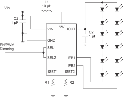 Figure 16. Driving up to 12 WLEDs With One LCD Backlight
space
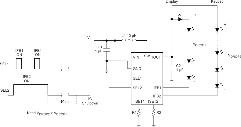 Figure 17. Driving A Keypad and LCD Backlight, Applying PWM Signal to the SEL1 Pin
