SLVSDY5E January   2018  – February 2024 TPS61322

PRODUCTION DATA  

  1.   1
  2. Features
  3. Applications
  4. Description
  5. Device Comparison Table
  6. Pin Configuration and Functions
    1.     Pin Functions
  7. Specifications
    1. 6.1 Absolute Maximum Ratings
    2. 6.2 ESD Ratings
    3. 6.3 Recommended Operating Conditions
    4. 6.4 Thermal Information
    5. 6.5 Electrical Characteristics
    6. 6.6 Typical Characteristics
  8. Detailed Description
    1. 7.1 Overview
    2. 7.2 Functional Block Diagram
    3. 7.3 Feature Description
      1. 7.3.1 Soft Start
      2. 7.3.2 Boost Controller Circuit
      3. 7.3.3 21
      4. 7.3.4 Undervoltage Lockout
      5. 7.3.5 Current Limit Operation
      6. 7.3.6 Overtemperature Protection
      7. 7.3.7 Device Functional Modes
  9. Application and Implementation
    1. 8.1 Application Information
    2. 8.2 Typical Application
      1. 8.2.1 Boost without Schottky Diode
        1. 8.2.1.1 Design Requirements
        2. 8.2.1.2 Detailed Design Procedure
          1. 8.2.1.2.1 Custom Design With WEBENCH® Tools
          2. 8.2.1.2.2 Maximum Output Current
          3. 8.2.1.2.3 Inductor Selection
          4. 8.2.1.2.4 35
          5. 8.2.1.2.5 Capacitor Selection
          6. 8.2.1.2.6 37
        3. 8.2.1.3 Application Curves
      2. 8.2.2 Boost with Schottky Diode
        1. 8.2.2.1 Design Requirements
        2. 8.2.2.2 Detailed Design Procedure
          1. 8.2.2.2.1 Inductor Selection
          2. 8.2.2.2.2 Schottky Diode Selection
          3. 8.2.2.2.3 Capacitor Selection
        3. 8.2.2.3 Application Curves
    3. 8.3 System Examples
      1. 8.3.1 Detail Design Schematics
  10. Power Supply Recommendations
  11. 10Layout
    1. 10.1 Layout Guidelines
    2. 10.2 Layout Examples
  12. 11Device and Documentation Support
    1. 11.1 Device Support
      1. 11.1.1 Third-Party Products Disclaimer
      2. 11.1.2 Development Support
        1. 11.1.2.1 Custom Design With WEBENCH® Tools
    2. 11.2 Documentation Support
      1. 11.2.1 Related Documentation
    3. 11.3 Receiving Notification of Documentation Updates
    4. 11.4 Support Resources
    5. 11.5 Trademarks
    6. 11.6 Electrostatic Discharge Caution
    7. 11.7 Glossary
  13. 12Revision History
  14. 13Mechanical, Packaging, and Orderable Information

Package Options

Mechanical Data (Package|Pins)
Thermal pad, mechanical data (Package|Pins)
Orderable Information

System Examples

TPS61322xx can be easily shut down with an external switch Q1 as shown in Figure 8-20. The switch can be mechanical switch, a P-channel MOSFET, or a PNP transistor. For a mechanical switch, there is no control logic circuit needed to turn on or turn off the switch.
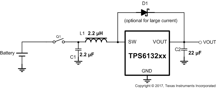
GUID-61947EDC-15EB-43A4-8737-618AA7F814D8-low.gif
Figure 8-20 True Shutdown for TPS61322xx