SLVSDY5E January   2018  – February 2024 TPS61322

PRODUCTION DATA  

  1.   1
  2. Features
  3. Applications
  4. Description
  5. Device Comparison Table
  6. Pin Configuration and Functions
    1.     Pin Functions
  7. Specifications
    1. 6.1 Absolute Maximum Ratings
    2. 6.2 ESD Ratings
    3. 6.3 Recommended Operating Conditions
    4. 6.4 Thermal Information
    5. 6.5 Electrical Characteristics
    6. 6.6 Typical Characteristics
  8. Detailed Description
    1. 7.1 Overview
    2. 7.2 Functional Block Diagram
    3. 7.3 Feature Description
      1. 7.3.1 Soft Start
      2. 7.3.2 Boost Controller Circuit
      3. 7.3.3 21
      4. 7.3.4 Undervoltage Lockout
      5. 7.3.5 Current Limit Operation
      6. 7.3.6 Overtemperature Protection
      7. 7.3.7 Device Functional Modes
  9. Application and Implementation
    1. 8.1 Application Information
    2. 8.2 Typical Application
      1. 8.2.1 Boost without Schottky Diode
        1. 8.2.1.1 Design Requirements
        2. 8.2.1.2 Detailed Design Procedure
          1. 8.2.1.2.1 Custom Design With WEBENCH® Tools
          2. 8.2.1.2.2 Maximum Output Current
          3. 8.2.1.2.3 Inductor Selection
          4. 8.2.1.2.4 35
          5. 8.2.1.2.5 Capacitor Selection
          6. 8.2.1.2.6 37
        3. 8.2.1.3 Application Curves
      2. 8.2.2 Boost with Schottky Diode
        1. 8.2.2.1 Design Requirements
        2. 8.2.2.2 Detailed Design Procedure
          1. 8.2.2.2.1 Inductor Selection
          2. 8.2.2.2.2 Schottky Diode Selection
          3. 8.2.2.2.3 Capacitor Selection
        3. 8.2.2.3 Application Curves
    3. 8.3 System Examples
      1. 8.3.1 Detail Design Schematics
  10. Power Supply Recommendations
  11. 10Layout
    1. 10.1 Layout Guidelines
    2. 10.2 Layout Examples
  12. 11Device and Documentation Support
    1. 11.1 Device Support
      1. 11.1.1 Third-Party Products Disclaimer
      2. 11.1.2 Development Support
        1. 11.1.2.1 Custom Design With WEBENCH® Tools
    2. 11.2 Documentation Support
      1. 11.2.1 Related Documentation
    3. 11.3 Receiving Notification of Documentation Updates
    4. 11.4 Support Resources
    5. 11.5 Trademarks
    6. 11.6 Electrostatic Discharge Caution
    7. 11.7 Glossary
  13. 12Revision History
  14. 13Mechanical, Packaging, and Orderable Information

Package Options

Mechanical Data (Package|Pins)
Thermal pad, mechanical data (Package|Pins)
Orderable Information

Description

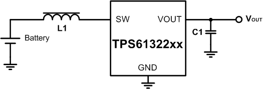
The TPS61322 is a synchronous boost converter with only 6.5-µA quiescent current. The TPS61322 provides a power-supply solution for products powered by alkaline battery, NiMH rechargeable battery, or one-cell Li-ion battery. The boost converter is based on a hysteretic control topology using synchronous rectification to obtain maximum efficiency at minimal quiescent current. The TPS61322 also allows the use of small external inductor and capacitors. Higher than 90% efficiency is achieved at 10-mA load from 1.5-V input to 2.2-V output conversion.

The TPS61322 can also support high output current applications with an external schottky diode. The TPS613222A provides higher than 500-mA output current capability at 3-V input voltage to 5-V output voltage conversion with an external Schottky diode in parallel with the internal rectifier FET.

The output voltage is set internally to a fixed output voltage from 1.8 V to 5.5 V in increments of 0.1 V. Thus, it only needs two external components to get the desired output voltage. The TPS61322 also implements thermal shutdown protection function.

The TPS61322 is available in a 2.9-mm × 1.3-mm 3-pin SOT package or a 2.9-mm × 1.6-mm 5-pin SOT package.

Device Information(1)
PART NUMBER PACKAGE BODY SIZE (NOM)
TPS61322 SOT-23 (3) 2.90 mm × 1.30 mm
SOT-23 (5) 2.90 mm × 1.60 mm
For all available packages, see the orderable addendum at the end of the data sheet.
GUID-8D11815F-B0DA-4C7F-AD51-A574AB850309-low.gifTypical Application Circuit