SLVS977B February 2010 – July 2016 TPS61325
PRODUCTION DATA.
- 1 Features
- 2 Applications
- 3 Description
- 4 Revision History
- 5 Device Comparison Table
- 6 Pin Configuration and Functions
- 7 Specifications
- 8 Parameter Measurement Information
-
9 Detailed Description
- 9.1 Overview
- 9.2 Functional Block Diagram
- 9.3
Feature Description
- 9.3.1 LED High-current Regulators, Unused Inputs
- 9.3.2 Safety Timer Accuracy
- 9.3.3 Current Limit Operation
- 9.3.4 Start-Up Sequence
- 9.3.5 Power Good (Flash Ready)
- 9.3.6 LED Temperature Monitoring
- 9.3.7 Hot Die Detector
- 9.3.8 Undervoltage Lockout
- 9.3.9 Storage Capacitor Active Cell Balancing
- 9.3.10 RED Light Privacy Indicator
- 9.3.11 White LED Privacy Indicator
- 9.3.12 Storage Capacitor, Precharge Voltage Calibration
- 9.3.13 Storage Capacitor, Adaptive Precharge Voltage
- 9.3.14 Serial Interface Description
- 9.4
Device Functional Modes
- 9.4.1 Down Mode In Voltage Regulation Mode
- 9.4.2 Power-Save Mode Operation, Efficiency
- 9.4.3 Mode Of Operation: DC-Light and Flashlight
- 9.4.4 Flash Strobe Is Level Sensitive (STT = 0): LED Strobe Follows STRB0 and STRB1 Inputs
- 9.4.5 Flash Strobe Is Leading Edge Sensitive (STT = 1): One-Shot LED Strobe
- 9.4.6 LED Failure Modes and Overvoltage Protection
- 9.4.7 Hardware Voltage Mode Selection
- 9.4.8 Flashlight Blanking (Tx-MASK)
- 9.4.9 Shutdown
- 9.4.10 Thermal Shutdown
- 9.5 Programming
- 9.6
Register Maps
- 9.6.1 Slave Address Byte
- 9.6.2 Register Address Byte
- 9.6.3 REGISTER0 (address = 0x00)
- 9.6.4 REGISTER1 (address = 0x01)
- 9.6.5 REGISTER2 (address = 0x02)
- 9.6.6 REGISTER3 (address = 0x03)
- 9.6.7 REGISTER4 (address = 0x04)
- 9.6.8 REGISTER5 (address = 0x05)
- 9.6.9 REGISTER6 (address = 0x06)
- 9.6.10 REGISTER7 (address = 0x07)
- 10Application and Implementation
- 11Power Supply Recommendations
- 12Layout
- 13Device and Documentation Support
- 14Mechanical, Packaging, and Orderable Information
Package Options
Mechanical Data (Package|Pins)
- YFF|20
Thermal pad, mechanical data (Package|Pins)
Orderable Information
10 Application and Implementation
NOTE
Information in the following applications sections is not part of the TI component specification, and TI does not warrant its accuracy or completeness. TI’s customers are responsible for determining suitability of components for their purposes. Customers should validate and test their design implementation to confirm system functionality.
10.1 Application Information
The TPS6132x drives up to three white LEDs in parallel. The extended high-current mode (HC_SEL) allows up to 1025-mA and 2050-mA, and 1025-mA flash current out of the storage capacitor. The high-capacity storage capacitor on the output of the boost regulator provides the high-peak flash LED current, thereby reducing the peak current demand from the battery to a minimum.
In the TPS6132x device, the DC-light and flash can be controlled either by the I2C interface or by the means of hardware control signals (STRB0 and STRB1). The maximum duration of the flashlight pulse can be limited by means of an internal user programmable safety timer (STIM). The DC-light watchdog timer can be disabled by pulling high the STRB1 signal.
10.2 Typical Applications
10.2.1 4100-mA Two White High-Power LED Flashlight With Storage Capacitor
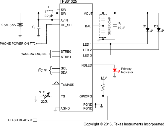 Figure 62. 4100-mA Two High-Power White LED Flashlight With Storage Capacitor Schematic
10.2.1.1 Design Requirements
In this application, the TPS61325 is required to drive a 4100-mA, two high-power white LED, flashlight with an input voltage range of 2.5 V to 5.5 V. This is a high-power LED application, so a storage capacitor is required to maintain sufficient headroom voltage across the LED current regulators for the entire strobe time and also minimize the power dissipation in the device.
10.2.1.2 Detailed Design Procedure
10.2.1.2.1 Inductor Selection
A boost converter requires two main passive components for storing energy during the conversion. A boost inductor and a storage capacitor at the output are required. The TPS6132x device integrates a current limit protection circuitry. The valley current of the PMOS rectifier is sensed to limit the maximum current flowing through the synchronous rectifier and the inductor. The valley peak current limit (250 mA, 1150 mA, 1600 mA) is user selectable through the I2C interface.
To optimize solution size the TPS6132x device is designed to operate with inductance values from 1.3 μH to 2.9 μH. TI recommends 2.2-µH inductance be used in typical high current white LED applications.
The highest peak current through the inductor and the power switch depends on the output load, the input and output voltages. Estimation of the maximum average inductor current and the maximum inductor peak current can be done using Equation 2 and Equation 3:


where
- f = switching frequency (2 MHz)
- L = inductance value (2.2 μH)
- η = estimated efficiency (85%)
The losses in the inductor caused by magnetic hysteresis losses and copper losses are a major parameter for total circuit efficiency.
Table 17. List of Inductors
| MANUFACTURER | SERIES | DIMENSIONS | ILIM SETTINGS |
|---|---|---|---|
| FDK | MIPST2520 | 2.5 mm x 2 mm x 0.8 mm (maximum) height | 250 mA (typical) |
| MIP2520 | 2.5 mm x 2 mm x 1 mm (maximum) height | ||
| MIPSA2520 | 2.5 mm x 2 mm x 1.2 mm (maximum) height | ||
| MURATA | LQM2HP-G0 | 2.5 mm x 2 mm x 1 mm (maximum) height | |
| LQM2HP-GC | 2.5 mm x 2 mm x 1 mm (maximum) height | ||
| TDK | VLF3014AT | 2.6 mm x 2.8 mm x 1.4 mm (maximum) height | 1150 mA (typical) |
| COILCRAFT | LPS3015 | 3 mm x 3 mm x 1.5 mm (maximum) height | |
| MURATA | LQH2HPN | 2.5 mm x 2 mm x 1.2 mm (maximum) height | |
| TOKO | FDSE0312 | 3 mm x 3 mm x 1.2 mm (maximum) height | 1600 mA (typical) |
| MURATA | LQM32PN | 3.2 mm x 2.5 mm x 1.2 mm (maximum) height |
10.2.1.2.2 Input Capacitor
TI recommends low ESR ceramic capacitors for good input voltage filtering. TI recommends a 10-μF input capacitor to improve transient behavior of the regulator and EMI behavior of the total power supply circuit. The input capacitor must be placed as close as possible to the input pin of the converter.
10.2.1.2.3 Output Capacitor
The major parameter necessary to define the output capacitor is the maximum allowed output voltage ripple of the converter. This ripple is determined by two parameters of the capacitor, the capacitance and the ESR. It is possible to calculate the minimum capacitance required for the defined ripple, supposing that the ESR is zero, by using Equation 4:

where
- f is the switching frequency
- ΔV is the maximum allowed ripple
With a chosen ripple voltage of 10 mV, a minimum capacitance of 10 μF is required. The total ripple is larger due to the ESR of the output capacitor. This additional component of the ripple can be calculated using Equation 5:
The total ripple is the sum of the ripple caused by the capacitance and the ripple caused by the ESR of the capacitor. Additional ripple is caused by load transients. This means that the output capacitor must completely supply the load during the charging phase of the inductor. A reasonable value of the output capacitance depends on the speed of the load transients and the load current during the load change.
For the standard current white LED application (HC_SEL = 0, TPS6132x), a minimum of 3-μF effective output capacitance is usually required when operating with 2.2-μH (typical) inductors. For solution size reasons, this is usually one or more X5R or X7R ceramic capacitors.
Depending on the material, size, and therefore margin to the rated voltage of the used output capacitor, degradation on the effective capacitance can be observed. This loss of capacitance is related to the DC bias voltage applied. TI recommends checking that the selected capacitors are showing enough effective capacitance under real operating conditions.
To support high-current camera flash application (HC_SEL = 1), the converter is designed to work with a low voltage super-capacitor on the output to take advantage of the benefits they offer. A low-voltage super-capacitor in the 0.1-F to 1.5-F range, and with ESR larger than 40 mΩ, is suitable in the TPS6132x application circuit. For this device the output capacitor must be connected between the VOUT pin and a good ground connection.
10.2.1.2.4 NTC Selection
The TPS6132x requires a negative thermistor (NTC) for sensing the LED temperature. Once the temperature monitoring feature is activated, a regulated bias current, approximately 24 μA, is driven out of the TS port and produce a voltage across the thermistor.
If the temperature of the NTC-thermistor rises due to the heat dissipated by the LED, the voltage on the TS input pin decreases. When this voltage goes below the warning threshold, the LEDWARN bit in REGISTER6 is set. This flag is cleared by reading the register.
If the voltage on the TS input decreases further and falls below hot threshold, the LEDHOT bit in REGISTER6 is set and the device automatically goes into shutdown mode to avoid damaging the LED. This status is latched until the LEDHOT flag gets cleared by software.
The selection of the NTC-thermistor value strongly depends on the power dissipated by the LED and all components surrounding the temperature sensor and on the cooling capabilities of each specific application. With a 220-kΩ (at 25°C) thermistor, the valid temperature window is set from 60°C to 90°C. The temperature window can be enlarged by adding external resistors to the TS pin application circuit. To ensure proper triggering of the LEDWARN and LEDHOT flags in noisy environments, the TS signal may require additional filtering capacitance.
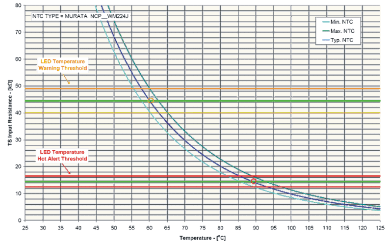 Figure 63. Temperature Monitoring Characteristic
Table 18. List of Negative Thermistor (NTC)
| MANUFACTURER | PART NUMBER | VALUE |
|---|---|---|
| MURATA | NCP18WM224J03RB | 220 kΩ |
10.2.1.2.5 Checking Loop Stability
The first step of circuit and stability evaluation is to look from a steady-state perspective at the following signals:
- Switching node (SW)
- Inductor current (IL)
- Output ripple voltage (VOUT(AC))
These are the basic signals that must be measured when evaluating a switching converter. When the switching waveform shows large duty cycle jitter or the output voltage or inductor current shows oscillations the regulation loop may be unstable. This is often a result of improper board layout or inductor and capacitor combinations.
The load transient response must be tested as a next step in the evaluation of the regulation loop. VOUT can be monitored for settling time, overshoot or ringing that helps judge the converter's stability. Without any ringing, the loop usually has more than 45° of phase margin.
Because the damping factor of the circuitry is directly related to several resistive parameters (for example, MOSFET rDS(on)) that are temperature dependant, the loop stability analysis must be done over the input voltage range, output current range, and temperature range.
10.2.1.3 Application Curves
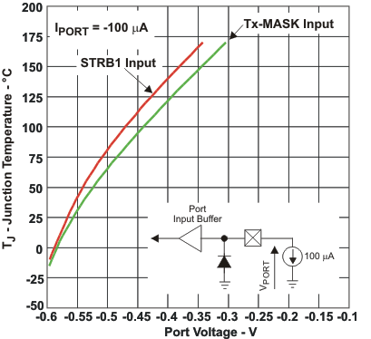 Figure 64. Junction Temperature vs Port Voltage
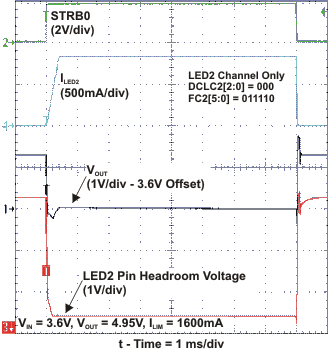 Figure 65. Flash Sequence (HC_SEL = 0)
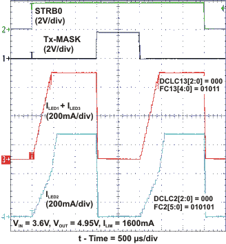 Figure 66. Tx-Masking Operation (HC_SEL = 0)
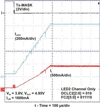 Figure 68. Tx-Masking Operation (HC_SEL = 0)
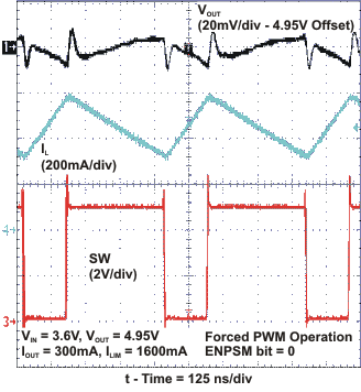 Figure 70. PWM Operation
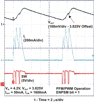 Figure 72. Down-Mode Operation (Voltage Mode)
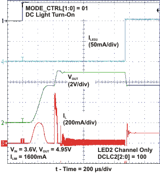 Figure 74. Start-Up Into DC-Light Operation
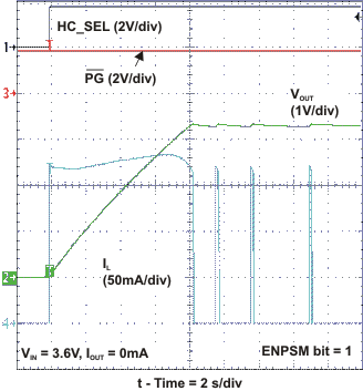 Figure 76. Storage Capacitor Precharge (HC_SEL = 1)
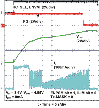 Figure 78. Storage Capacitor Charge-Up (HC_SEL = 1)
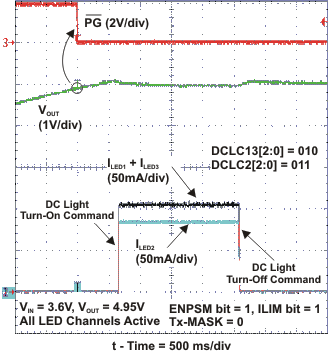 Figure 80. DC-Light Operation (HC_SEL = 1)
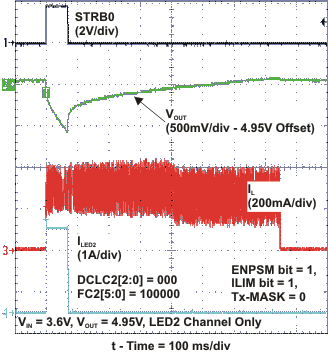 Figure 82. Flash Sequence (HC_SEL = 1)
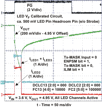 Figure 84. Flash Sequence (HC_SEL = 1)
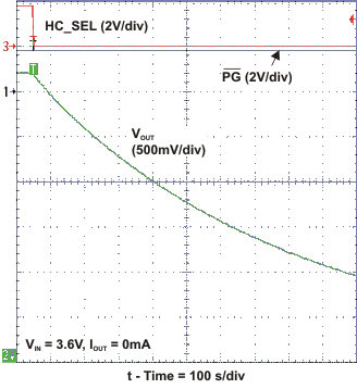 Figure 86. Shutdown (HC_SEL = 1)
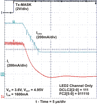 Figure 67. Tx-Masking Operation (HC_SEL = 0)
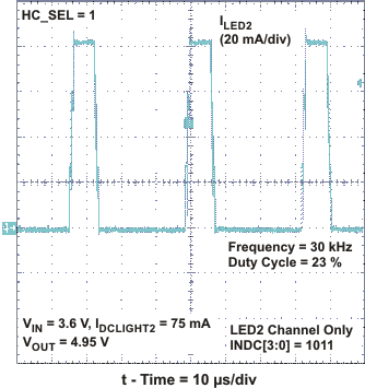 Figure 69. Low-LIGHT Dimming Mode Operation
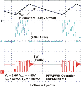 Figure 71. PFM Operation
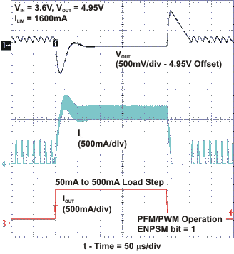 Figure 73. Voltage Mode Load Transient Response
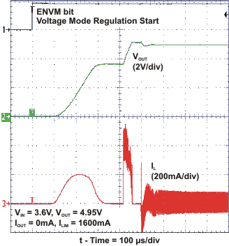 Figure 75. Start-Up Into Voltage Mode Operation
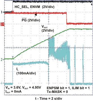 Figure 77. Storage Capacitor Charge-Up (HC_SEL = 1)
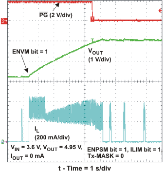 Figure 79. Storage Capacitor Charge-Up (HC_SEL = 1)
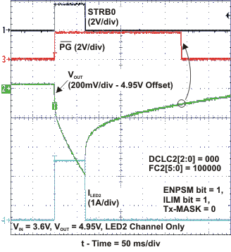 Figure 81. Flash Sequence (HC_SEL = 1)
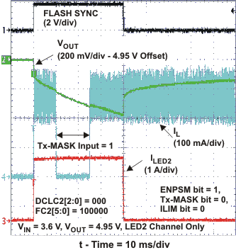 Figure 83. Flash Sequence (HC_SEL = 1)
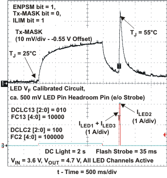 Figure 85. Junction Temperature Monitoring (HC_SEL = 1)
10.2.2 Other Application Circuit Examples
Figure 87 and Figure 88 show application circuit examples using the TPS61325 device. Customers must fully validate and test these circuits before implementing a design based on these examples.
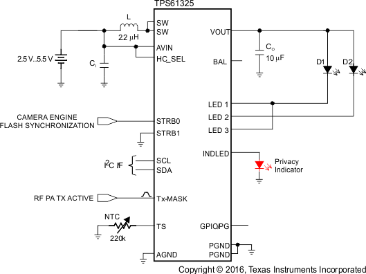 Figure 87. 2x 600-mA High Power White LED Solution With Privacy Indicator Schematic
In this application, TPS61325 is used to drive two 600-mA white LEDs. A storage capacitor is not necessary because the LED current can be supplied by the TPS61325 directly. The privacy indicator is turned on.
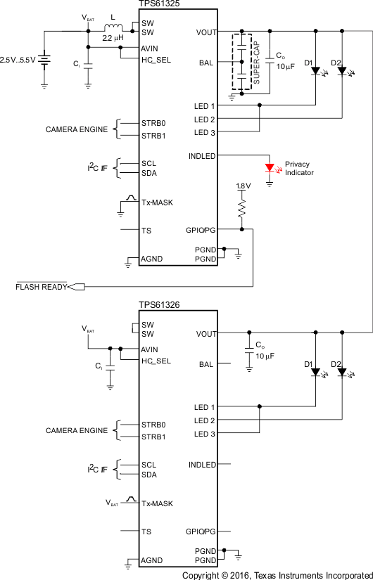 Figure 88. 8200-mA Four High-Power White LED Flashlight With Storage Capacitor Schematic
In this application, it is required to drive a 8200-mA, four high-power white LED, flashlight. Because it is beyond the driving capability of the TPS61325, two devices are connected in parallel to drive the LED flashlight. One works as a master with a storage capacitor, and the other works as a slave.