SLVS681F June 2006 – August 2014 TPS62400 , TPS62401 , TPS62402 , TPS62403 , TPS62404
PRODUCTION DATA.
- 1 Features
- 2 Applications
- 3 Description
- 4 Revision History
- 5 Device Options
- 6 Pin Configuration and Functions
- 7 Specifications
- 8 Detailed Description
-
9 Application and Implementation
- 9.1 Application Information
- 9.2
Typical Applications
- 9.2.1
TPS6240x, Dual Outputs Step Down Converter
- 9.2.1.1 Design Requirements
- 9.2.1.2
Detailed Design Procedure
- 9.2.1.2.1 Converter1 Adjustable Default Output Voltage Setting: TPS62400
- 9.2.1.2.2 Converter1 Fixed Default Output Voltage Setting (TPS62401, TPS62402, TPS62403, TPS62404).
- 9.2.1.2.3 Converter 2 Adjustable Default Output Voltage Setting TPS62400:
- 9.2.1.2.4 Converter 2 Fixed Default Output Voltage Setting
- 9.2.1.2.5 Output Filter Design (Inductor and Output Capacitor)
- 9.2.1.3 Application Curves
- 9.2.2 Various Output Voltages
- 9.2.3 Dynamic Voltage Scaling on Converter 1 by DEF_1 Pin
- 9.2.1
TPS6240x, Dual Outputs Step Down Converter
- 10Power Supply Recommendations
- 11Layout
- 12Device and Documentation Support
- 13Mechanical, Packaging, and Orderable Information
Package Options
Mechanical Data (Package|Pins)
- DRC|10
Thermal pad, mechanical data (Package|Pins)
- DRC|10
Orderable Information
6 Pin Configuration and Functions
DRC Package
10 Pins
Top View
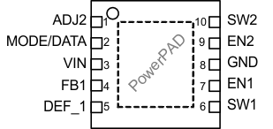
Pin Functions
| PIN | I/O | DESCRIPTION | ||
|---|---|---|---|---|
| NAME | NO. | |||
| ADJ2 | 1 | I | Input to adjust output voltage of converter 2. In adjustable version (TPS62400) connect a external resistor divider between VOUT2, this pin and GND to set output voltage between 0.6V and VIN. At fixed output voltage version (TPS62401, TPS62402, TPS62403, TPS62404) this pin MUST be directly connected to the output. If EasyScale Interface is used for converter 2, this pin must be directly connected to the output, too. | |
| DEF_1 | 5 | I | This pin defines the output voltage of converter 1. The pin acts either as analog input for output voltage setting via external resistors (TPS62400), or digital input to select between two fixed default output voltages (TPS62401, TPS62402, TPS62403, TPS62404). | |
| For the TPS62400, an external resistor network needs to be connected to this pin to adjust the default output voltage. | ||||
| Using the fixed output voltage device options this pin selects between two fixed default output voltages, see table ordering information | ||||
| EN1 | 7 | I | Enable Input for Converter1, active high | |
| EN2 | 9 | I | Enable Input for Converter 2, active high | |
| FB1 | 4 | I | Direct feedback voltage sense input of converter 1, connect directly to Vout 1. An internal feed forward capacitor is connected between this pin and the error amplifier. In case of fixed output voltage versions or when the Interface is used, this pin is connected to an internal resistor divider network. | |
| GND | 8 | GND for both converters; connect this pin to the PowerPAD™ | ||
| MODE/DATA | 2 | I/O | This Pin has 2 functions: | |
| 1. | Operation Mode selection: With low level, Power Save Mode is enabled where the device operates in PFM mode at light loads and enters automatically PWM mode at heavy loads. Pulling this PIN to high forces the device to operate in PWM mode over the whole load range. | |||
| 2. | EasyScale™ Interface function: One wire serial interface to change the output voltage of both converters. The pin has an open drain output to provide an acknowledge condition if requested. The current into the open drain output stage may not exceed 500μA. The interface is active if either EN1 or EN2 is high. | |||
| PowerPAD™ | Connect to GND | |||
| SW1 | 6 | I/O | Switch Pin of Converter 1. Connect to Inductor | |
| SW2 | 10 | I/O | Switch Pin of Converter 2. Connect to Inductor. | |
| VIN | 3 | Supply voltage, connect to VBAT, 2.5V to 6V | ||