SLVSEW4 April   2019 TPS650002-Q1

PRODUCTION DATA.  

  1. Features
  2. Applications
  3. Description
    1.     Device Images
      1.      Typical Application Schematic
  4. Revision History
  5. Pin Configuration and Functions
    1.     Pin Functions
  6. Specifications
    1. 6.1 Absolute Maximum Ratings
    2. 6.2 ESD Ratings
    3. 6.3 Recommended Operating Conditions
    4. 6.4 Thermal Information
    5. 6.5 Electrical Characteristics
    6. 6.6 Switching Characteristics
    7. 6.7 Typical Characteristics
  7. Detailed Description
    1. 7.1 Overview
    2. 7.2 Functional Block Diagram
    3. 7.3 Feature Description
      1. 7.3.1 Step-Down Converter
      2. 7.3.2 Soft Start
      3. 7.3.3 Linear Regulators
      4. 7.3.4 Power Good
    4. 7.4 Device Functional Modes
  8. Application and Implementation
    1. 8.1 Application Information
    2. 8.2 Typical Application
      1. 8.2.1 Design Requirements
      2. 8.2.2 Detailed Design Procedure
        1. 8.2.2.1 Output Filter Design (Inductor and Output Capacitor)
          1. 8.2.2.1.1 Inductor Selection
          2. 8.2.2.1.2 Output Capacitor Selection
        2. 8.2.2.2 Input Capacitor Selection
      3. 8.2.3 Application Curves
  9. Power Supply Recommendations
  10. 10Layout
    1. 10.1 Layout Guidelines
    2. 10.2 Layout Examples
  11. 11Device and Documentation Support
    1. 11.1 Device Support
      1. 11.1.1 Third-Party Products Disclaimer
    2. 11.2 Documentation Support
      1. 11.2.1 Related Documentation
    3. 11.3 Receiving Notification of Documentation Updates
    4. 11.4 Community Resources
    5. 11.5 Trademarks
    6. 11.6 Electrostatic Discharge Caution
    7. 11.7 Glossary
  12. 12Mechanical, Packaging, and Orderable Information

Package Options

Mechanical Data (Package|Pins)
Thermal pad, mechanical data (Package|Pins)
Orderable Information

Linear Regulators

The two linear dropout regulators (LDOs) in the TPS650002-Q1 are designed to provide flexibility in system design. Each LDO has a separate voltage input and enable signal. The input can be tied to the output of the step-down converter or the output of another voltage source. Each LDO output discharges to ground automatically when EN_LDOx goes low.

The LDOs are general-purpose devices that can handle inputs from 6 V down to 1.6 V. Figure 19 shows the necessary connections for LDO1. The same architecture applies to LDO2.
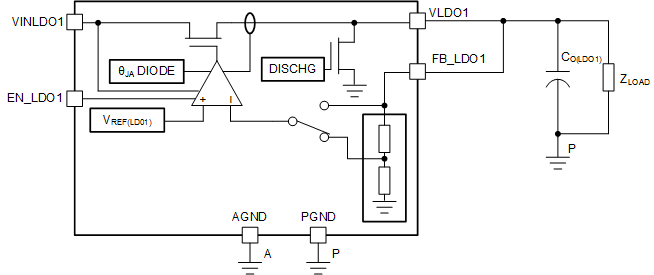
TPS650002-Q1 Fixed-LDO.gifFigure 19. LDO Block Diagram