SLVS754D March 2007 – January 2015 TPS65053
PRODUCTION DATA.
- 1 Features
- 2 Applications
- 3 Description
- 4 Revision History
- 5 Pin Configuration and Functions
- 6 Specifications
-
7 Detailed Description
- 7.1 Overview
- 7.2 Functional Block Diagrams
- 7.3 Feature Description
- 7.4 Device Functional Modes
-
8 Application and Implementation
- 8.1 Application Information
- 8.2
Typical Application
- 8.2.1 Design Requirements
- 8.2.2 Detailed Design Procedure
- 8.2.3 Application Curves
- 9 Power Supply Recommendations
- 10Layout
- 11Device and Documentation Support
- 12Mechanical, Packaging, and Orderable Information
Package Options
Mechanical Data (Package|Pins)
- RGE|24
Thermal pad, mechanical data (Package|Pins)
- RGE|24
Orderable Information
7 Detailed Description
7.1 Overview
The TPS6505xx include two synchronous step-down converters. The converters operate with 2.25 MHz fixed frequency pulse width modulation (PWM) at moderate to heavy load currents. At light load currents the converters automatically enter Power Save Mode and operate with PFM (Pulse Frequency Modulation).
During PWM operation the converters use a unique fast response voltage mode controller scheme with input voltage feed-forward to achieve good line and load regulation allowing the use of small ceramic input and output capacitors. At the beginning of each clock cycle initiated by the clock signal, the P-channel MOSFET switch is turned on and the inductor current ramps up until the comparator trips and the control logic turns off the switch. The current limit comparator will also turn off the switch in case the current limit of the P-channel switch is exceeded. After the adaptive dead time prevents shoot through current, the N-channel MOSFET rectifier is turned on and the inductor current ramps down. The next cycle is initiated by the clock signal again turning off the N-channel rectifier and turning on the P-channel switch.
The two DC-DC converters operate synchronized to each other, with converter 1 as the master. A 180 ° phase shift between Converter 1 and Converter 2 decreases the input RMS current. Therefore smaller input capacitors can be used.
The converters output voltage is set by an external resistor divider connected to FB_DCDC1 or FB_DCDC2, respectively. See Application and Implementation for more details.
7.2 Functional Block Diagrams
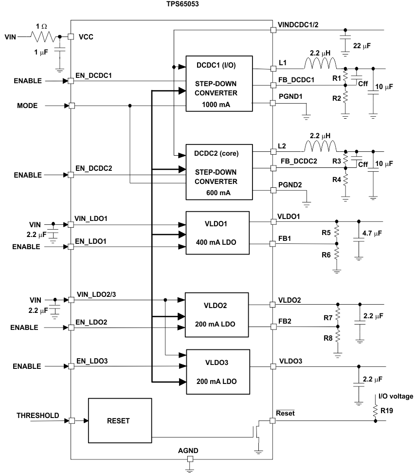
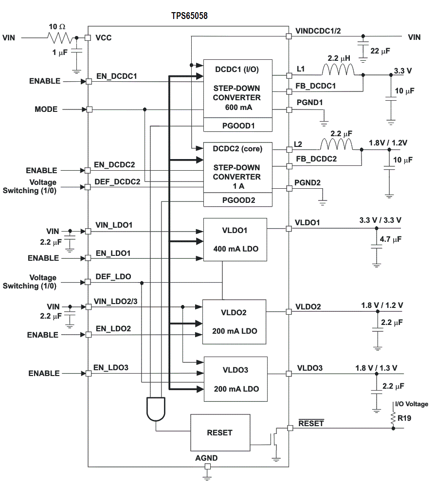 Figure 20. TPS65058 Functional Block Diagram
7.3 Feature Description
7.3.1 Power Save Mode
The Power Save Mode is enabled with Mode Pin set to low. If the load current decreases, the converters will enter Power Save Mode operation automatically. During Power Save Mode the converters operate with reduced switching frequency in PFM mode and with a minimum quiescent current to maintain high efficiency. The converter will position the output voltage typically 1% above the nominal output voltage. This voltage positioning feature minimizes voltage drops caused by a sudden load step.
In order to optimize the converter efficiency at light load the average current is monitored and if in PWM mode the inductor current remains below a certain threshold, then Power Save Mode is entered. The typical threshold can be calculated according to:
Average output current threshold to enter PFM mode:

Average output current threshold to leave PFM mode:

During the Power Save Mode the output voltage is monitored with a comparator. As the output voltage falls below the skip comparator threshold (skip comp) of VOUTnominal +1%, the P-channel switch will turn on and the converter effectively delivers a constant current as defined above. If the load is below the delivered current then the output voltage will rise until the same threshold is crossed again, whereupon all switching activity ceases, hence reducing the quiescent current to a minimum until the output voltage has dropped below the threshold again. If the load current is greater than the delivered current then the output voltage will fall until it crosses the skip comparator low (Skip Comp Low) threshold set to 1% below nominal Vout, whereupon Power Save Mode is exited and the converter returns to PWM mode.
These control methods reduce the quiescent current typically to 12μA per converter and the switching frequency to a minimum thereby achieving the highest converter efficiency. The PFM mode operates with very low output voltage ripple. The ripple depends on the comparator delay and the size of the output capacitor; increasing capacitor values will make the output ripple tend to zero.
The Power Save Mode can be disabled by driving the MODE pin high. Both converters will operate in fixed PWM mode. Power Save Mode Enable/Disable applies to both converters.
7.3.1.1 Dynamic Voltage Positioning
This feature reduces the voltage under/overshoots at load steps from light to heavy load and vice versa. It is activated in Power Save Mode operation when the converter runs in PFM Mode. It provides more headroom for both the voltage drop at a load step increase and the voltage increase at a load throw-off. This improves load transient behavior.
At light loads, in which the converters operate in PFM Mode, the output voltage is regulated typically 1% higher than the nominal value. In case of a load transient from light load to heavy load, the output voltage will drop until it reaches the skip comparator low threshold set to –1% below the nominal value and enters PWM mode. During a load throw off from heavy load to light load, the voltage overshoot is also minimized due to active regulation turning on the N-channel switch.
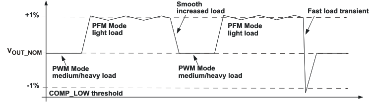 Figure 21. Dynamic Voltage Positioning
7.3.1.2 Soft Start
The two converters have an internal soft start circuit that limits the inrush current during start-up. During soft start, the output voltage ramp up is controlled as shown in Figure 22.
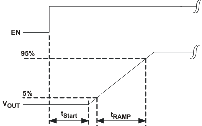 Figure 22. Soft Start
7.3.1.3 100% Duty Cycle Low Dropout Operation
The converters offer a low input to output voltage difference while still maintaining operation with the use of the 100% duty cycle mode. In this mode the P-channel switch is constantly turned on. This is particularly useful in battery-powered applications to achieve longest operation time by taking full advantage of the whole battery voltage range, i.e. The minimum input voltage to maintain regulation depends on the load current and output voltage and can be calculated as:

where
- Ioutmax = maximum output current plus inductor ripple current
- RDSonmax = maximum P-channel switch rDS(on)
- RL = DC resistance of the inductor
- Voutmax = nominal output voltage plus maximum output voltage tolerance
With decreasing load current, the device automatically switches into pulse skipping operation in which the power stage operates intermittently based on load demand. By running cycles periodically the switching losses are minimized and the device runs with a minimum quiescent current maintaining high efficiency.
In power save mode the converter only operates when the output voltage trips below its nominal output voltage. It ramps up the output voltage with several pulses and goes again into power save mode once the output voltage exceeds the nominal output voltage.
7.3.1.4 Undervoltage Lockout
The undervoltage lockout circuit prevents the device from malfunctioning by disabling the converter at low input voltages and from excessive discharge of the battery. The undervoltage lockout threshold is typically 1.8 V, max 2 V.
7.3.2 Mode Selection
The MODE pin allows mode selection between forced PWM Mode and power Save Mode for both converters. Connecting this pin to GND enables the automatic PWM and power save mode operation. The converters operate in fixed frequency PWM mode at moderate to heavy loads and in the PFM mode during light loads, maintaining high efficiency over a wide load current range.
Pulling the MODE pin high forces both converters to operate constantly in the PWM mode even at light load currents. The advantage is the converters operate with a fixed frequency that allows simple filtering of the switching frequency for noise sensitive applications. In this mode, the efficiency is lower compared to the power save mode during light loads. For additional flexibility it is possible to switch from power save mode to forced PWM mode during operation. This allows efficient power management by adjusting the operation of the converter to the specific system requirements.
7.3.3 Enable
The devices have a separate enable pin for each of the DCDC converters and for each of the LDO to start up independently. If EN_DCDC1, EN_DCDC2, EN_LDO1, EN_LDO2, EN_LDO3 are set to high, the corresponding converter starts up with soft start as previously described.
Pulling the enable pin low forces the device into shutdown, with a shutdown quiescent current as defined in the electrical characteristics. In this mode, the P and N-Channel MOSFETs are turned-off, the and the entire internal control circuitry is switched-off. If disabled, the outputs of the LDOs are pulled low by internal 350-Ω resistors, actively discharging the output capacitor. For proper operation the enable pins must be terminated and must not be left unconnected.
7.3.4 Dynamic Ouput Voltage Scaling
The TPS65058 has the feature: dynamic voltage scaling intended for core processor supply. The voltage scaling can be used for any application or to simply select the output voltage. The following description applies only to TPS65058.
The output voltage of the DCDC Converter 2 can be selected by a logic level on pin DEF_DCDC2. The output voltage can be changed dynamically during operation. The slew rate of the change of output voltage is controlled on DCDC2 to be 9.6mV/μs.
The output voltages on the LDOs can also be changed dynamically between two voltages by changing the logic level on pin DEF_LDO.
The output voltage options are:
Table 2. Output Voltage Selection
| DEF_LDO | 1 | 0 |
|---|---|---|
| LDO1 | 3.3 V | 3.3 V |
| LDO2 | 1.8 V | 1.2 V |
| LDO3 | 1.8 V | 1.3 V |
| DEF_DCDC2 | 1 | 0 |
| DCDC2 | 1.8 V | 1.2 V |
7.3.5 RESET on the TPS65053x
The TPS65053x contain circuitry that can generate a reset pulse for a processor with a 100 ms delay time. The input voltage at a comparator is sensed at an input called THRESHOLD. When the voltage exceeds the 1V threshold, the output goes high after a 100 ms delay time. This circuitry is functional as soon as the supply voltage at Vcc exceeds the undervoltage lockout threshold. The RESET circuitry is active even if all DCDC converters and LDOs are disabled.
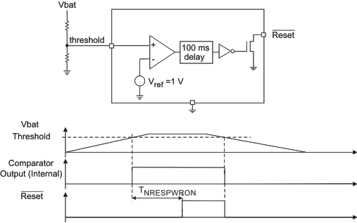 Figure 23. RESET Pulse Circuit for TPS65053x
7.3.6 RESET Generation and Output Monitoring on the TPS65058
The TPS65058 contains a monitor circuitry that monitors the outputs of the DCDC converters and applies a reset pulse to the RESET pin. As soon as the supply voltage on the VCC pin is above the undervoltage lockout threshold, the RESET pin is pulled low. After the enabling of both DCDC converters, the output voltages are monitored. When both outputs are within 95% of the desired output voltage, the reset timer is started and after a delay of 100ms the Reset output is switched to high impedance. If one of the output voltages is outside of the regulation band (90% of the desired value) the RESET pin remains to be pulled to ground. After both outputs are back in regulation, the 100ms timer is started, and after 100ms the RESET output is again switched to high impedance.
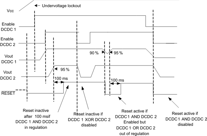 Figure 24. RESET Pulse Circuit for TPS65058
7.3.7 Short-Circuit Protection
All outputs are short circuit protected with a maximum output current as defined in the Electrical Characteristics.
7.3.8 Thermal Shutdown
As soon as the junction temperature, TJ, exceeds typically 150°C for the DCDC converters, the device goes into thermal shutdown. In this mode, the P and N-Channel MOSFETs are turned-off. The device continues its operation when the junction temperature falls below the thermal shutdown hysteresis again. A thermal shutdown for one of the DCDC converters will disable both converters simultaneously.
The thermal shutdown temperature for the LDOs are set to typically 140°C. Therefore a LDO which may be used to power an external voltage will never heat up the chip high enough to turn off the DCDC converters. If one LDO exceeds the thermal shutdown temperature, all LDOs will turn off simultaneously.
7.4 Device Functional Modes
This device has only one functional mode which is ON. The device enters this state if the device is within the operational VIN range on the VCC pin. The converters and LDOs can be enabled and/or disabled in this state.