SLVS754D March 2007 – January 2015 TPS65053
PRODUCTION DATA.
- 1 Features
- 2 Applications
- 3 Description
- 4 Revision History
- 5 Pin Configuration and Functions
- 6 Specifications
-
7 Detailed Description
- 7.1 Overview
- 7.2 Functional Block Diagrams
- 7.3 Feature Description
- 7.4 Device Functional Modes
-
8 Application and Implementation
- 8.1 Application Information
- 8.2
Typical Application
- 8.2.1 Design Requirements
- 8.2.2 Detailed Design Procedure
- 8.2.3 Application Curves
- 9 Power Supply Recommendations
- 10Layout
- 11Device and Documentation Support
- 12Mechanical, Packaging, and Orderable Information
Package Options
Mechanical Data (Package|Pins)
- RGE|24
Thermal pad, mechanical data (Package|Pins)
- RGE|24
Orderable Information
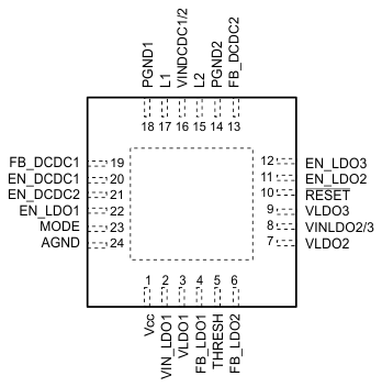
5 Pin Configuration and Functions
RGE Package - TPS65053x
24 Pins
Top View
RGE Package - TPS65058
24 Pins
Top View
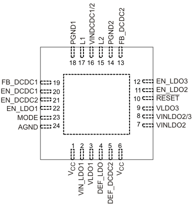
Pin Functions
| PIN | I/O | DESCRIPTION | ||
|---|---|---|---|---|
| NAME | TPS65053, TPS650531, TPS650532 | TPS65058 | ||
| AGND | 24 | 24 | I | Analog GND, connect to PGND and PowerPAD™ |
| DEF_DCDC2 | — | 5 | I | Switches output votlage at DCDC2, logic HIGH = 1.8V, logic LOW = 1.2V |
| DEF_LDO | — | 4 | I | Switches output votlage at LDO2, logic HIGH = 1.8V, logic LOW = 1.2V |
| Switches output votlage at LDO3, logic HIGH = 1.8V, logic LOW = 1.3V | ||||
| EN_DCDC1 | 20 | 20 | I | Enable Input for converter 1, active high |
| EN_DCDC2 | 21 | 21 | I | Enable Input for converter 2, active high |
| EN_LDO1 | 22 | 22 | I | Enable input for LDO1. Logic high enables the LDO, logic low disables the LDO. |
| EN_LDO2 | 11 | 11 | I | Enable input for LDO2. Logic high enables the LDO, logic low disables the LDO. |
| EN_LDO3 | 12 | 12 | I | Enable input for LDO3. Logic high enables the LDO, logic low disables the LDO. |
| FB_DCDC1 | 19 | 19 | I | Input to adjust output voltage of converter 1 between 0.6 V and VI. Connect external resistor divider between VOUT1, this pin and GND. |
| FB_DCDC2 | 13 | 13 | I | Input to adjust output voltage of converter 2 between 0.6V and VIN. Connect external resistor divider between VOUT2, this pin and GND. |
| FB_LDO1 | 4 | — | 1 | Feedback input for the external voltage divider. |
| FB_LDO2 | 6 | — | I | Feedback input for the external voltage divider. |
| L1 | 17 | 17 | O | Switch pin of converter 1. Connected to Inductor |
| L2 | 15 | 15 | O | Switch Pin of converter 2. Connected to Inductor. |
| MODE | 23 | 23 | I | Select between Power Save Mode and forced PWM Mode for DCDC1 and DCDC2. In Power Save Mode, PFM is used at light loads, PWM for higher loads. If PIN is set to high level, forced PWM Mode is selected. If Pin has low level, then the device operates in Power Save Mode. |
| PGND1 | 18 | 18 | I | GND for converter 1 |
| PGND2 | 14 | 14 | I | GND for converter 2 |
| PowerPAD™ | — | — | — | Connect to GND |
| VCC | 1 | 1, 6 | I | Power supply for digital and analog circuitry of DCDC1, DCDC2 and LDOs. This pin must be connected to the same voltage supply as VINDCDC1/2. |
| VINDCDC1/2 | 16 | 16 | I | Input voltage for VDCDC1 and VDCDC2 step-down converter. This must be connected to the same voltage supply as VCC. |
| VINLDO1 | 2 | 2 | I | Input voltage for LDO1 |
| VINLDO2/3 | 8 | 8 | I | Input voltage for LDO2 and LDO3 |
| VLDO1 | 3 | 3 | O | Output voltage of LDO1 |
| VLDO2 | 7 | 7 | O | Output voltage of LDO2 |
| VLDO3 | 9 | 9 | O | Output voltage of LDO3 |
| THRESHOLD | 5 | — | I | Reset input |
| RESET | 10 | 10 | O | Open drain active low reset output, 100 ms reset delay time. |