SLVS754D March 2007 – January 2015 TPS65053
PRODUCTION DATA.
- 1 Features
- 2 Applications
- 3 Description
- 4 Revision History
- 5 Pin Configuration and Functions
- 6 Specifications
-
7 Detailed Description
- 7.1 Overview
- 7.2 Functional Block Diagrams
- 7.3 Feature Description
- 7.4 Device Functional Modes
-
8 Application and Implementation
- 8.1 Application Information
- 8.2
Typical Application
- 8.2.1 Design Requirements
- 8.2.2 Detailed Design Procedure
- 8.2.3 Application Curves
- 9 Power Supply Recommendations
- 10Layout
- 11Device and Documentation Support
- 12Mechanical, Packaging, and Orderable Information
Package Options
Mechanical Data (Package|Pins)
- RGE|24
Thermal pad, mechanical data (Package|Pins)
- RGE|24
Orderable Information
10 Layout
10.1 Layout Guidelines
- The input capacitors for the DCDC converters should be placed as close as possible to the VINDCDC1/2 pin and the PGND1 and PGND2 pins.
- The inductor of the output filter should be placed as close as possible to the device to provide the shortest switch node possible, reducing the noise emitted into the system and increasing the efficiency.
- Sense the feedback voltage from the output at the output capacitors to ensure the best DC accuracy. Feedback should be routed away from noisey sources such as the inductor. If possible route on the opposing side as the swiitch node and inductor and place a GND plane between the feedback and the noisey sources or keepout underneath them entirely.
- Place the output capacitors as close as possible to the inductor to reduce the feedback loop as much as possible. This will ensure best regulation at the feedback point.
- Place the device as close as possible to the the most demanding or sensitive load. The output capacitors should be placed close to the input of the load. This will ensure the best AC performance possible.
- The input and output capacitors for the LDOs should be placed close to the device for best regulation performance.
- The use a one common ground plane is recommended for the device layout. The AGND can be separated from the PGND but, a large low parasitic PGND is required to connect the PGNDx pins to the CIN and external PGND connections.
10.2 Layout Example
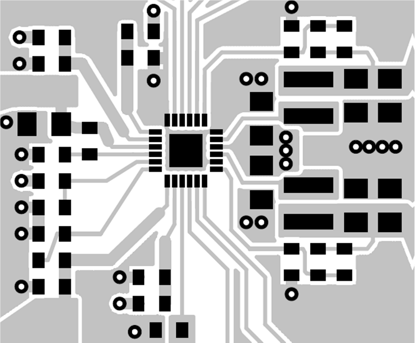 Figure 28. Layout Example Schematic for TPS65053