SLVSE48C january 2018 – may 2023 TPS65268-Q1
PRODUCTION DATA
- 1
- 1 Features
- 2 Applications
- 3 Description
- 4 Revision History
- 5 Pin Configuration and Functions
- 6 Specifications
-
7 Detailed Description
- 7.1 Overview
- 7.2 Functional Block Diagram
- 7.3
Feature Description
- 7.3.1 Adjusting the Output Voltage
- 7.3.2 Enable and Adjusting UVLO
- 7.3.3 Soft-Start Time
- 7.3.4 Power-Up Sequencing
- 7.3.5 V7V Low-Dropout Regulator and Bootstrap
- 7.3.6 Out-of-Phase Operation
- 7.3.7 Output Overvoltage Protection (OVP)
- 7.3.8 Slope Compensation
- 7.3.9 Overcurrent Protection
- 7.3.10 Power Good
- 7.3.11 Thermal Shutdown
- 7.4 Device Functional Modes
- 8 Application and Implementation
- 9 Device and Documentation Support
- 10Mechanical, Packaging, and Orderable Information
Package Options
Mechanical Data (Package|Pins)
- RHB|32
Thermal pad, mechanical data (Package|Pins)
- RHB|32
Orderable Information
7.3.10.1 Adjustable Switching Frequency
The ROSC pin can be used to set the switching frequency by connecting a resistor to ground. The switching frequency of the device is adjustable from 200 kHz to 2.3 MHz.
To determine the ROSC resistance for a given switching frequency, use Equation 6 or the curve in Figure 7-10. To reduce the solution size, the user must set the switching frequency as high as possible, but consider tradeoffs of the supply efficiency and minimum controllable on-time.
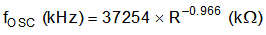
 Figure 7-10 ROSC vs Switching Frequency
When an external clock applies to ROSC pin, the internal PLL has been implemented to allow internal clock synchronizing to an external clock from 200 kHz to 2300 kHz. To implement the clock synchronization feature, connect a square-wave clock signal to the ROSC pin with a duty cycle from 20% to 80%. The clock signal amplitude must transition lower than 0.4 V and higher than 2.0 V. The start of the switching cycle is synchronized to the falling edge of ROSC pin.
In applications where both resistor mode and synchronization mode are needed, the user can configure the device as shown in Figure 7-11. Before an external clock is present, the device works in resistor mode and the ROSC resistor sets the switching frequency. When an external clock is present, the synchronization mode overrides the resistor mode. The first time the ROSC pin is pulled above the ROSC high threshold (2 V), the device switches from the resistor mode to the synchronization mode and the ROSC pin is in the high impedance state as the PLL starts to lock onto the frequency of the external clock. TI does not recommend switching from the synchronization mode back to the resistor mode because the internal switching frequency drops to 100 kHz first before returning to the switching frequency set by ROSC resistor.
 Figure 7-11 Works With Resistor Mode and Synchronization Mode