SLVSAX7E August 2011 – August 2016 TPS65270
PRODUCTION DATA.
- 1 Features
- 2 Applications
- 3 Description
- 4 Revision History
- 5 Description (continued)
- 6 Pin Configuration and Functions
- 7 Specifications
- 8 Detailed Description
- 9 Application and Implementation
- 10Power Supply Recommendations
- 11Layout
- 12Device and Documentation Support
- 13Mechanical, Packaging, and Orderable Information
Package Options
Mechanical Data (Package|Pins)
Thermal pad, mechanical data (Package|Pins)
Orderable Information
8 Detailed Description
8.1 Overview
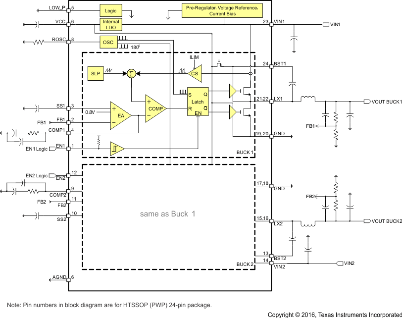
TPS65270 is a power management IC with two step-down buck converters. Both high-side and low-side MOSFETs are integrated to provide fully synchronous conversion with higher efficiency. TPS65270 can support 4.5-V to 18-V input supply, 2-A continuous current for Buck 1 and 3 A for Buck 2. The buck converters have an automatic PSM mode, which can improve power dissipation during light loads. Alternatively, the device implements a constant frequency mode by connecting the LOW_P pin to ground. The wide switching frequency of 300 kHz to 1.4 MHz allows for efficiency and size optimization. The switching frequency is adjustable by selecting a resistor to ground on the ROSC pin. Input ripple is reduced by 180° out-of-phase operation between Buck 1 and Buck 2.
Both buck converters have peak current mode control which simplifies the loop compensation. A traditional type II compensation network can stabilize the system and achieve fast transient response. Moreover, an optional capacitor in parallel with the upper resistor of the feedback divider provides one more zero and makes the crossover frequency over 100 kHz. Each buck converter has an individual cycle-by-cycle current limit and low side reverse current limit.
The device has a built-in LDO regulator. During a standby mode, the 6.5-V LDO can be used to drive MCU and other active loads. with this LDO, system is able to turn off the two buck converters so as to reduce the power consumption and improve the standby efficiency. Each converter has its own programmable soft start that can reduce the input inrush current. The individual Enable pins for each independent control of each output voltage and power sequence.
8.2 Functional Block Diagram

8.3 Feature Description
8.3.1 Adjustable Switching Frequency
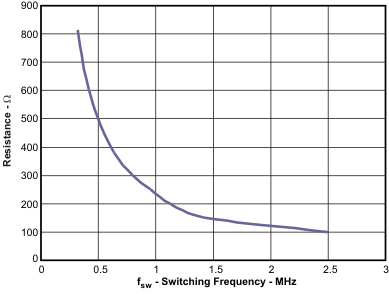
To select the internal switching frequency connect a resistor from ROSC to ground. Figure 7 shows the required resistance for a given switching frequency.
 Figure 7. ROSC vs Switching Frequency

For operation at 800 kHz, a 300-kΩ resistor is required.
8.3.2 Out-of-Phase Operation
To reduce input ripple current, Buck 1 and Buck 2 operate 180° out-of-phase. This enables the system having less input ripple, then to lower component cost, save board space and reduce EMI.
8.3.3 Delayed Start-Up
If a delayed start-up is required on any of the buck converters fit a ceramic capacitor to the ENx pins. The delay added is approximately 0.75 ms per nF connected to the pin. The EN pins have a weak 1-MΩ pullup to the 5-V rail.
8.3.4 Soft-Start Time
The device has an internal pullup current source of 5 µA that charges an external slow start capacitor to implement a slow start time. Equation 2 shows how to select a slow start capacitor based on an expected slow start time. The voltage reference (VREF) is 0.8 V and the slow start charge current (Iss) is 5 µA. The soft-start circuit requires 1 nF per 160 µs to be connected at the SS pin. An 800-µs soft-start time is implemented for all converters fitting 4.7 nF to the relevant pins.

8.3.5 Adjusting the Output Voltage
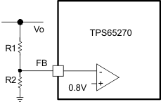
The output voltage is set with a resistor divider from the output node to the FB pin. TI recommends using divider resistors of 1% tolerance or better. To improve efficiency at light load, start with 40.2 kΩ for the R1 resistor and use the Equation 3 to calculate R2.

 Figure 8. Voltage Divider Circuit
8.3.6 Error Amplifier
The device has a transconductance error amplifier. The transconductance of the error amplifier is 130 µA/V during normal operation. The frequency compensation network is connected between the COMP pin and ground.
8.3.7 Slope Compensation
The device has a built-in slope compensation ramp. The slope compensation can prevent subharmonic oscillations in peak current mode control when duty cycle becomes too large.
8.3.8 Overcurrent Protection
The current through the internal high-side MOSFET is sampled and scaled through an internal pilot device during the hig time. The sampled current is compared to overcurrent limit. If the peak inductor current exceeds the overcurrent limit reference level, an internal overcurrent fault counter is set to 1 and an internal flag is set. The internal power MOSFET is immediately turned off and is not turned on again until the next switching cycle. The protection circuitry continues to monitor the current and turns off the internal MOSFET as described. If the overcurrent condition persists for four sequential clock cycles, the overcurrent fault counter overflows indicating an overcurrent fault condition exists. The regulator is shut down and power good goes low. If the overcurrent condition clears before the counter reaches four consecutive cycles, the internal flag and counter are reset. The protection circuitry attempts to recover from the overcurrent condition after waiting four soft-start cycles. The internal overcurrent flag and counter are reset. A normal soft-start cycle is attempted and normal operation continues if the fault condition has cleared. If the overcurrent fault counter overflows during soft start, the converter shuts down and this hiccup mode operation repeats.
8.3.9 Thermal Shutdown
The device implements an internal thermal shutdown to protect itself if the junction temperature exceeds 160°C. The thermal shutdown forces the device to stop switching when the junction temperature exceeds thermal trip threshold. Once the die temperature decreases below 140°C, the device reinitiates the power up sequence. The thermal shutdown hysteresis is 20°C.
8.3.10 Low Power Mode Operation
By pulling the Low_P pin high all converters operate in pulse-skipping mode, greatly reducing the overall power consumption at light and no load conditions. When LOW_P is tied to low, all converters run in forced PWM mode.
8.4 Device Functional Modes
8.4.1 Operation With Minimum VIN (VIN < 4.45 V)
The device will operate with input voltages above the 4.45-V UVLO maximum voltage. The typical UVLO voltage is 4.2 V and the device may operate at input voltage above this point. The device may also operate with lower input voltages; the minimum UVLO voltage is 4 V (rising) and 3.65 V (falling). The device will not operate with input voltages below the UVLO minimum voltage.
8.4.2 Operation With EN Control
The enable rising edge threshold voltage is 1.55 V (minimum) and falling edge threshold voltage is 0.4 V (maximum). With EN held below 0.4 V the device is disabled and switching is inhibited. The IC quiescent current is reduced in this state. The device becomes active when input voltage is above the UVLO threshold and the EN voltage is increased above 1.55 V. Switching is enabled and the internal soft-start sequence is initiated as shown in Figure 13.