SLVSAX7E August 2011 – August 2016 TPS65270
PRODUCTION DATA.
- 1 Features
- 2 Applications
- 3 Description
- 4 Revision History
- 5 Description (continued)
- 6 Pin Configuration and Functions
- 7 Specifications
- 8 Detailed Description
- 9 Application and Implementation
- 10Power Supply Recommendations
- 11Layout
- 12Device and Documentation Support
- 13Mechanical, Packaging, and Orderable Information
Package Options
Mechanical Data (Package|Pins)
Thermal pad, mechanical data (Package|Pins)
Orderable Information
11 Layout
11.1 Layout Guidelines
Layout is a critical portion of PMIC designs.
- Place VOUT, and LX on the top layer and an inner power plane for VIN.
- Fit also on the top layer connections for the remaining pins of the PMIC and a large top side area filled with ground.
- The top layer ground area sould be connected to the bottom ground layer(s) using vias at the input bypass capacitor, the output filter cpacitor and directly under the TPS65270 device to provide a thermal path from the Powerpad land to ground.
- The AGND pin must be tied directly to the power pad under the IC and the power pad.
- For operation at full rated load, the top side ground area together with the bottom ground plane, must provide adequate heat dissipating area.
- There are several signals paths that conduct fast changing currents or voltages that can interact with stray inductance or parasitic capacitance to generate noise or degrade the power supplies performance. To help eliminate these problems, the VIN pin must be bypassed to ground with a low ESR ceramic bypass capacitor with X5R or X7R dielectric. Minimize the loop area formed by the bypass capacitor connections, the VIN pins, and the ground connections. Because the LX connection is the switching node, the output inductor must be placed close to the LX pins, and the area of the PCB conductor minimized to prevent excessive capacitive coupling.
- The output filter capacitor ground must use the same power ground trace as the VIN input bypass capacitor. Try to minimize this conductor length while maintaining adequate width.
- The compensation must be as close as possible to the COMP pins. The COMP and OSC pins are sensitive to noise so the components associated to these pins must be placed as close as possible to the IC and routed with minimal lengths of trace.
11.2 Layout Example
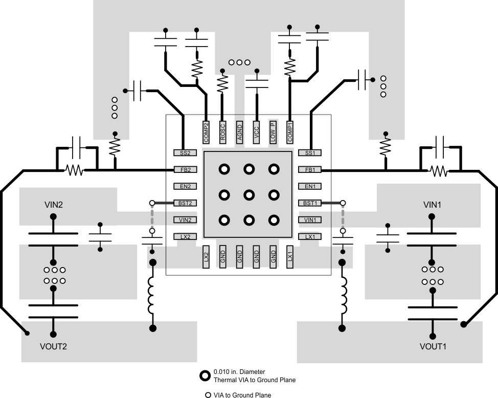 Figure 18. Example Layout for the TPS65270
11.3 Power Dissipation
The total power dissipation inside TPS65270 must not exceed the maximum allowable junction temperature of 125°C to maintain reliable operation. The maximum allowable power dissipation is a function of the thermal resistance of the package (RθJA) and ambient temperature.
To calculate the temperature inside the device under continuous loading use the following procedure.
- Define the set voltage for each converter.
- Define the continuous loading on each converter. Make sure do not exceed the converter maximum loading.
- Determine from the graphs below the expected losses in watts per converter inside the device. The losses depend on the input supply, the selected switching frequency, the output voltage and the converter chosen.
- To calculate the maximum temperature inside the IC use the following formula:
- PDIS is the sum of losses in all converters
- RθJA is the junction to ambient thermal impedance of the device and it is heavily dependant on board layout
Equation 14. 

where
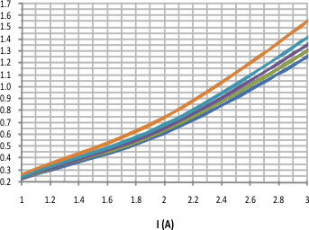
| VIN = 12 V | fSW = 500 kHz |
| VOUT (from top to bottom) = 5 V, 3.3 V, 2.5 V, 1.8 V, 1.2 V | |
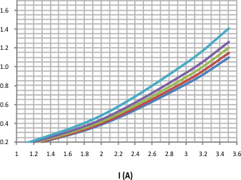
| VIN = 12 V | fSW = 500 kHz |
| VOUT (from top to bottom) = 5 V, 3.3 V, 2.5 V, 1.8 V, 1.2 V | |
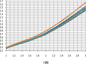
| VIN = 12 V | fSW = 1.1 MHz |
| VOUT (from top to bottom) = 5 V, 3.3 V, 2.5 V, 1.8 V, 1.2 V | |
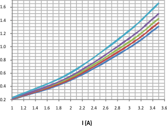
| VIN = 12 V | fSW = 1.1 MHz |
| VOUT (from top to bottom) = 5 V, 3.3 V, 2.5 V, 1.8 V, 1.2 V | |