SBVS047I April   2004  – November 2023 TPS715A

PRODUCTION DATA  

  1.   1
  2. Features
  3. Applications
  4. Description
  5. Pin Configuration and Functions
  6. Specifications
    1. 5.1 Absolute Maximum Ratings
    2. 5.2 ESD Ratings
    3. 5.3 Recommended Operating Conditions
    4. 5.4 Thermal Information
    5. 5.5 Electrical Characteristics
    6. 5.6 Typical Characteristics
  7. Detailed Description
    1. 6.1 Overview
    2. 6.2 Functional Block Diagrams
    3. 6.3 Feature Description
      1. 6.3.1 Wide Supply Range
      2. 6.3.2 Low Supply Current
      3. 6.3.3 Current Limit
      4. 6.3.4 Dropout Voltage (VDO)
    4. 6.4 Device Functional Modes
      1. 6.4.1 Normal Operation
      2. 6.4.2 Dropout Operation
  8. Application and Implementation
    1. 7.1 Application Information
    2. 7.2 Typical Applications
      1. 7.2.1 Design Requirements
      2. 7.2.2 Detailed Design Procedure
        1. 7.2.2.1 Setting VOUT for the TPS715A01 Adjustable LDO
        2. 7.2.2.2 External Capacitor Requirements
        3. 7.2.2.3 Input and Output Capacitor Requirements
        4. 7.2.2.4 Reverse Current
        5. 7.2.2.5 Feed-Forward Capacitor (CFF)
        6. 7.2.2.6 Power Dissipation (PD)
        7. 7.2.2.7 Estimating Junction Temperature
      3. 7.2.3 Application Curves
    3. 7.3 Best Design Practices
    4. 7.4 Power Supply Recommendations
    5. 7.5 Layout
      1. 7.5.1 Layout Guidelines
        1. 7.5.1.1 Power Dissipation
      2. 7.5.2 Layout Example
  9. Device and Documentation Support
    1. 8.1 Device Support
      1. 8.1.1 Development Support
        1. 8.1.1.1 Evaluation Module
        2. 8.1.1.2 Spice Models
      2. 8.1.2 Device Nomenclature
    2. 8.2 Documentation Support
      1. 8.2.1 Related Documentation
    3. 8.3 Receiving Notification of Documentation Updates
    4. 8.4 Support Resources
    5. 8.5 Trademarks
    6. 8.6 Electrostatic Discharge Caution
    7. 8.7 Glossary
  10. Revision History
  11. 10Mechanical, Packaging, and Orderable Information

Package Options

Refer to the PDF data sheet for device specific package drawings

Mechanical Data (Package|Pins)
  • DRV|6
  • DRB|8
Thermal pad, mechanical data (Package|Pins)
Orderable Information

Power Dissipation

To provide reliable operation, worst-case junction temperature must not exceed 125°C. This restriction limits the power dissipation the regulator can handle in any given application. To make sure the junction temperature is within acceptable limits, calculate the maximum allowable dissipation, PD(max), and the actual dissipation, PD, which must be less than or equal to PD(max).

The maximum-power-dissipation limit is determined using Equation 11.
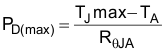
Equation 11. GUID-A7414963-F2CD-473F-B2E4-8FEC9707EB0A-low.gif

where:

  • TJmax is the maximum allowable junction temperature
  • RθJA is the thermal resistance junction-to-ambient for the package (see the Thermal Information table)
  • TA is the ambient temperature

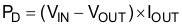
The regulator power dissipation is calculated using Equation 12.

Equation 12. GUID-A0C34900-FD2A-4CE5-BEE1-161D53E261A7-low.gif

For a higher power package version of the TPS715A, see the TPS715A.