for all voltage versions at TJ = 25°C, VIN = VOUT(nom) + 1 V, IOUT = 10 mA, VEN = 2.2 V, and COUT = 2.2 μF (unless otherwise noted)
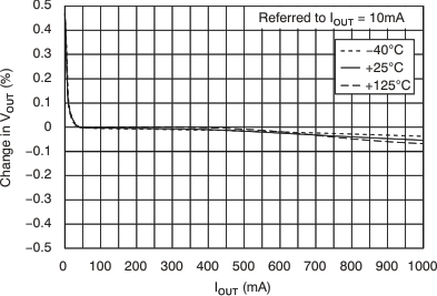
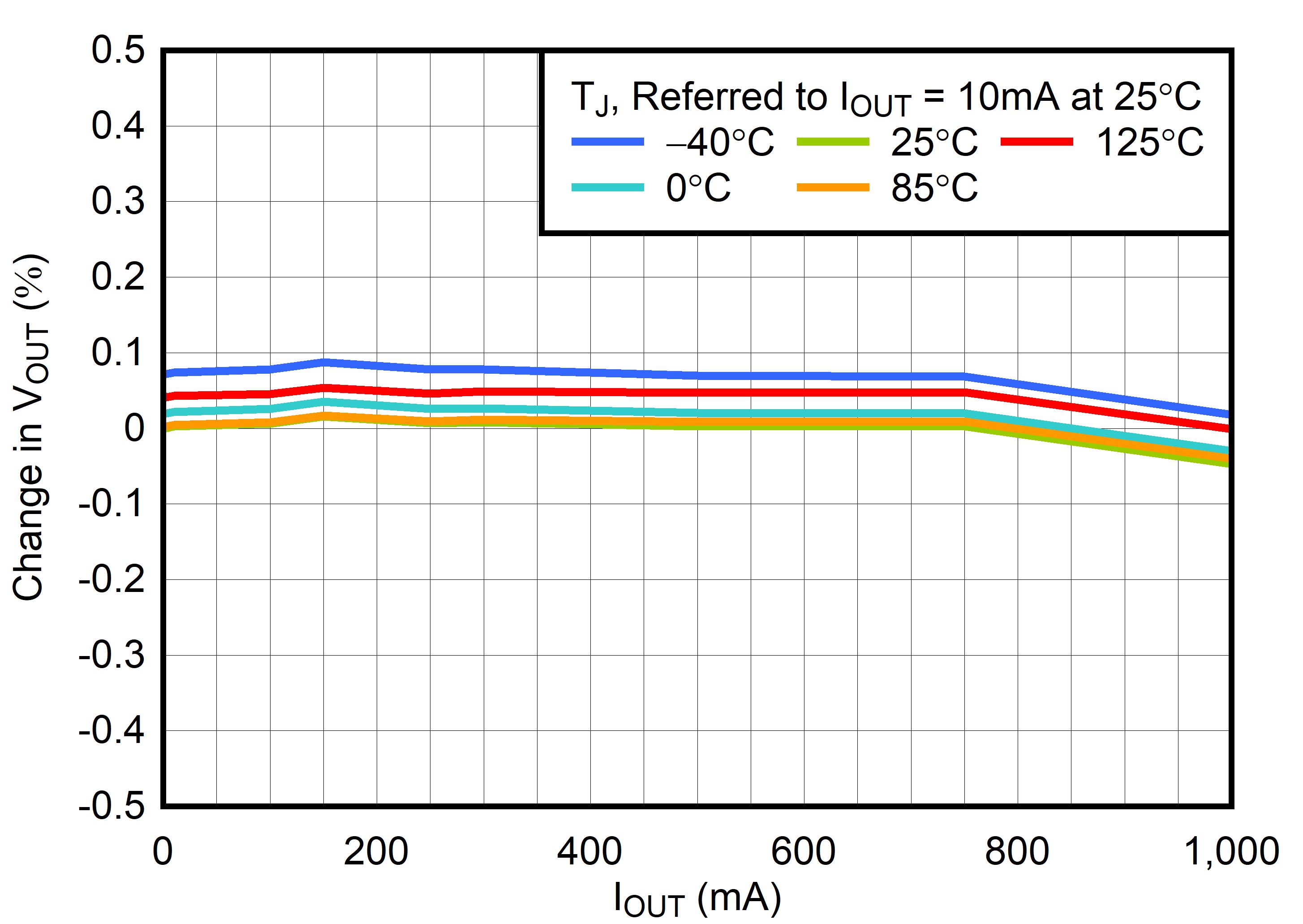
 Figure 5-1 Load Regulation
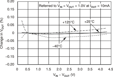
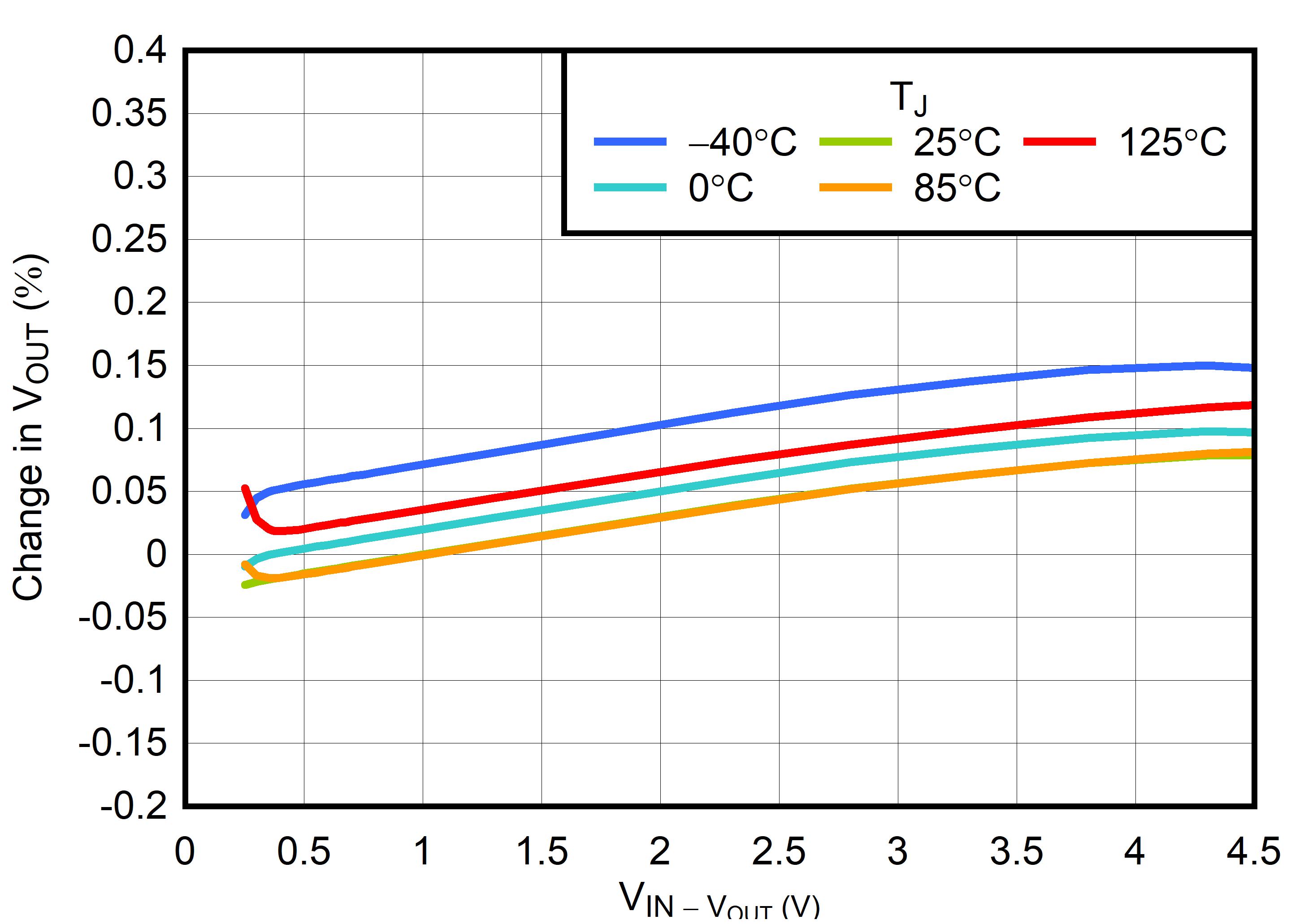
 Figure 5-3 Line Regulation
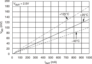
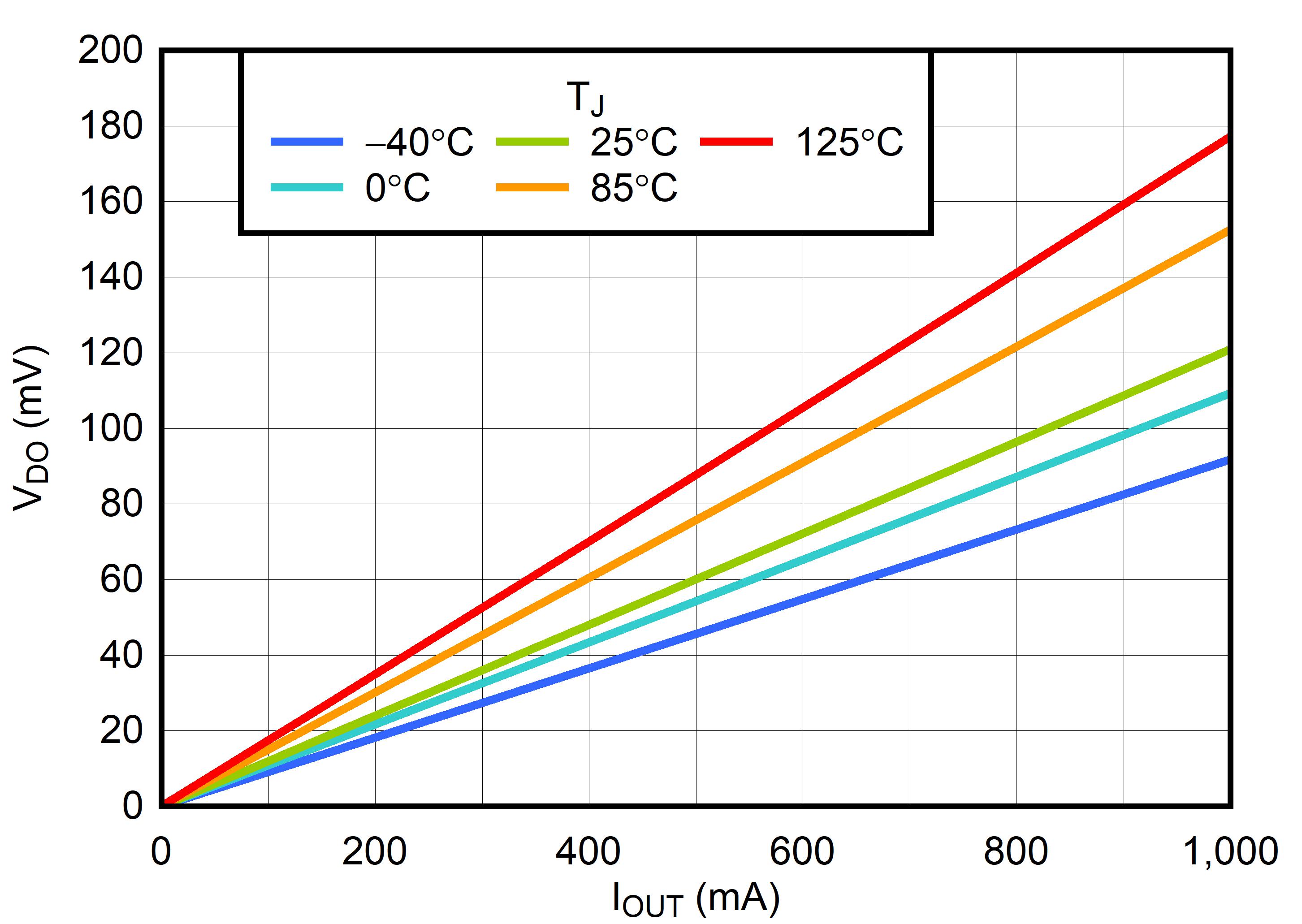
 Figure 5-5 Dropout Voltage vs Output Current
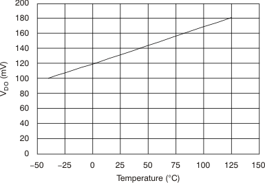
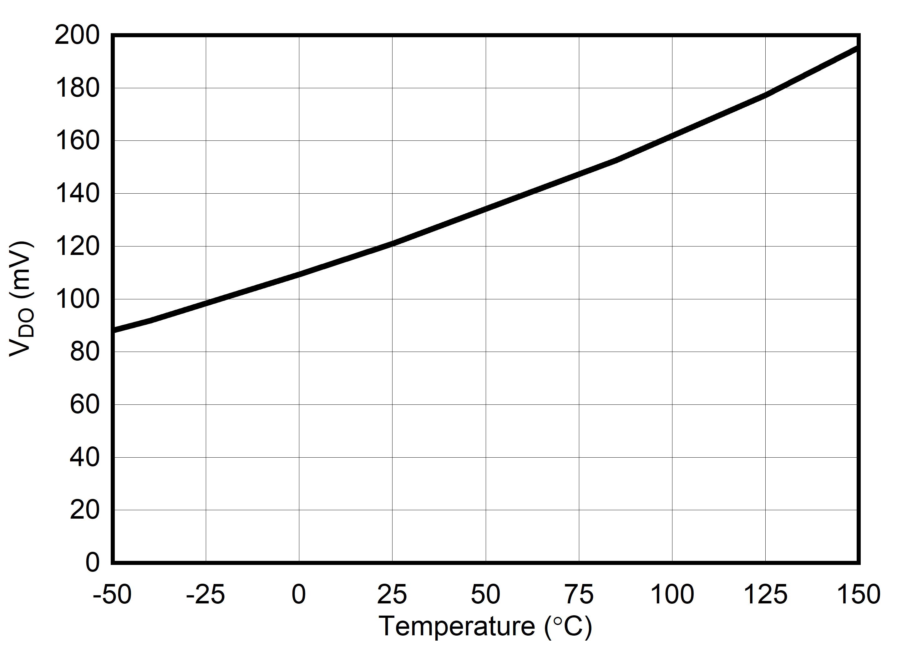
 Figure 5-7 Dropout Voltage vs Temperature
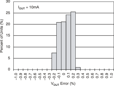
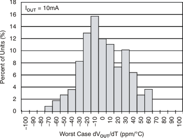
 Figure 5-9 Output Voltage Histogram
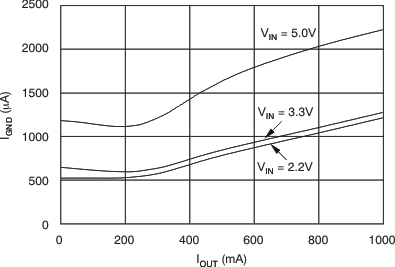
 Figure 5-11 Ground Pin Current vs Output Current
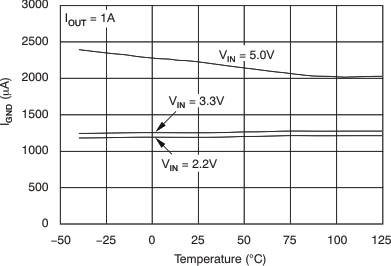
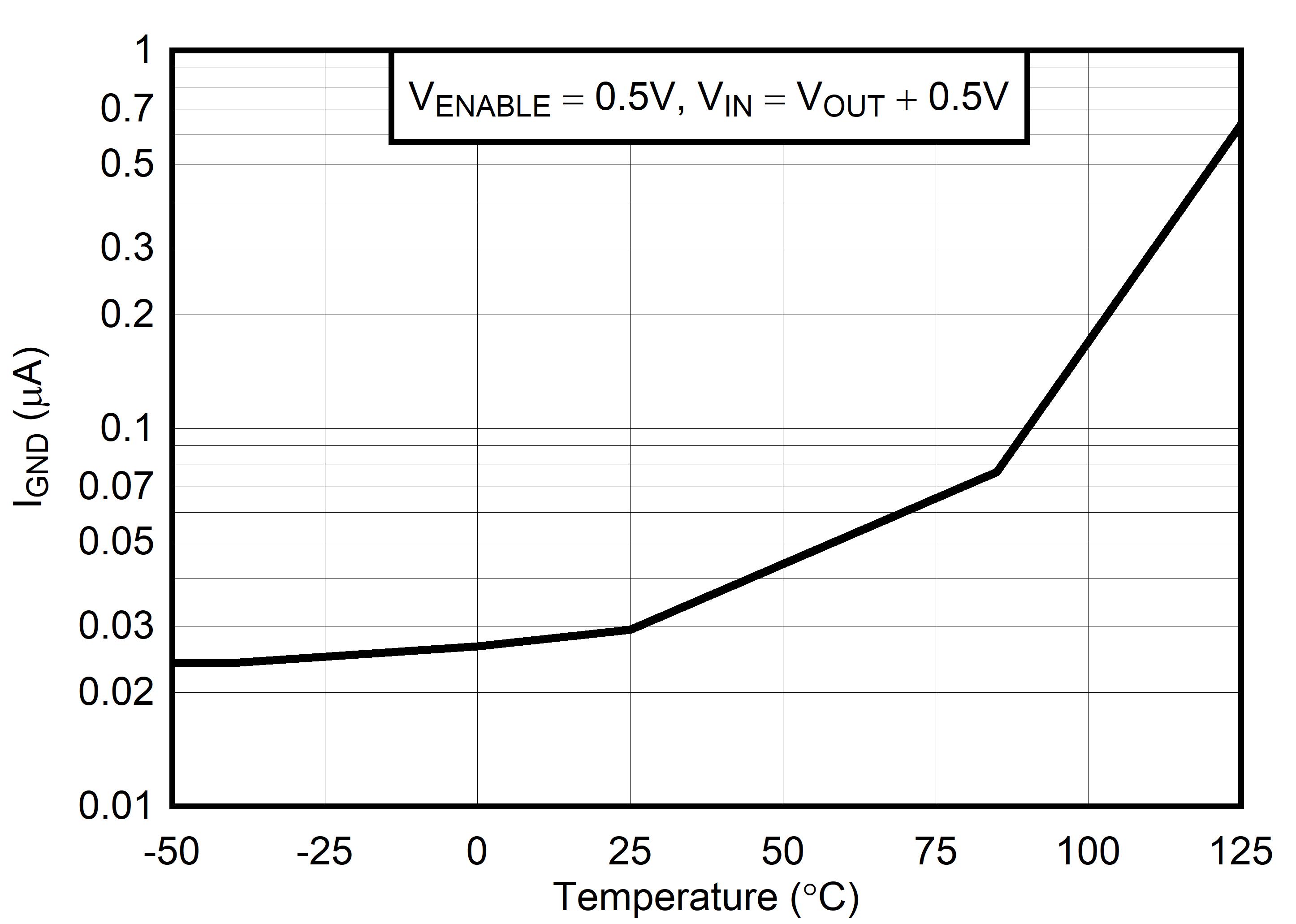
 Figure 5-13 Ground Pin Current vs Temperature
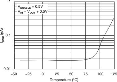
 Figure 5-15 Ground Pin Current in Shutdown vs Temperature
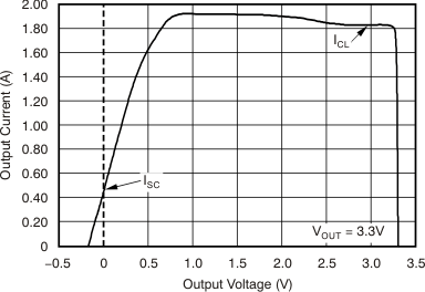
 Figure 5-17 Current Limit vs VOUT (Foldback)
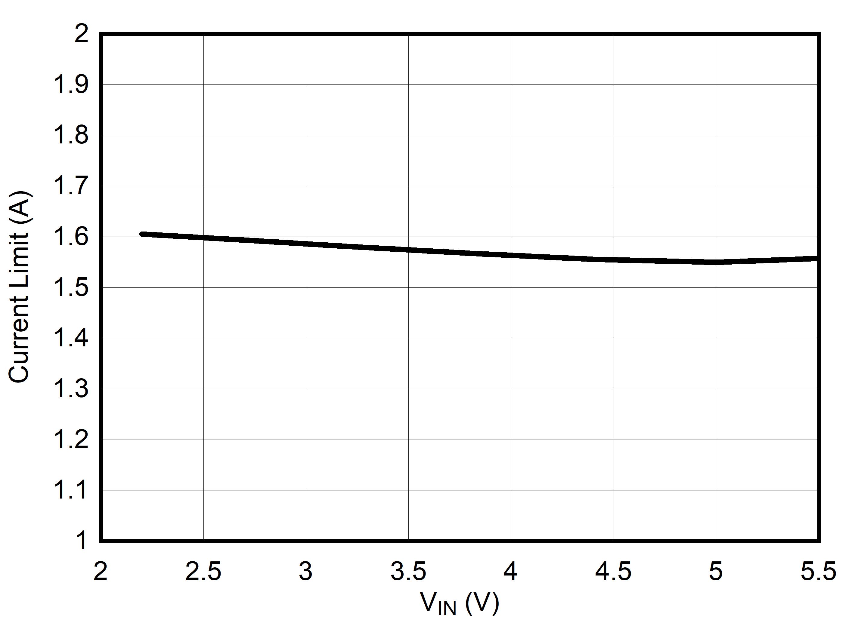
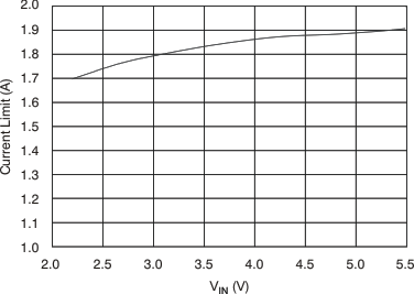
 Figure 5-19 Current Limit vs VIN
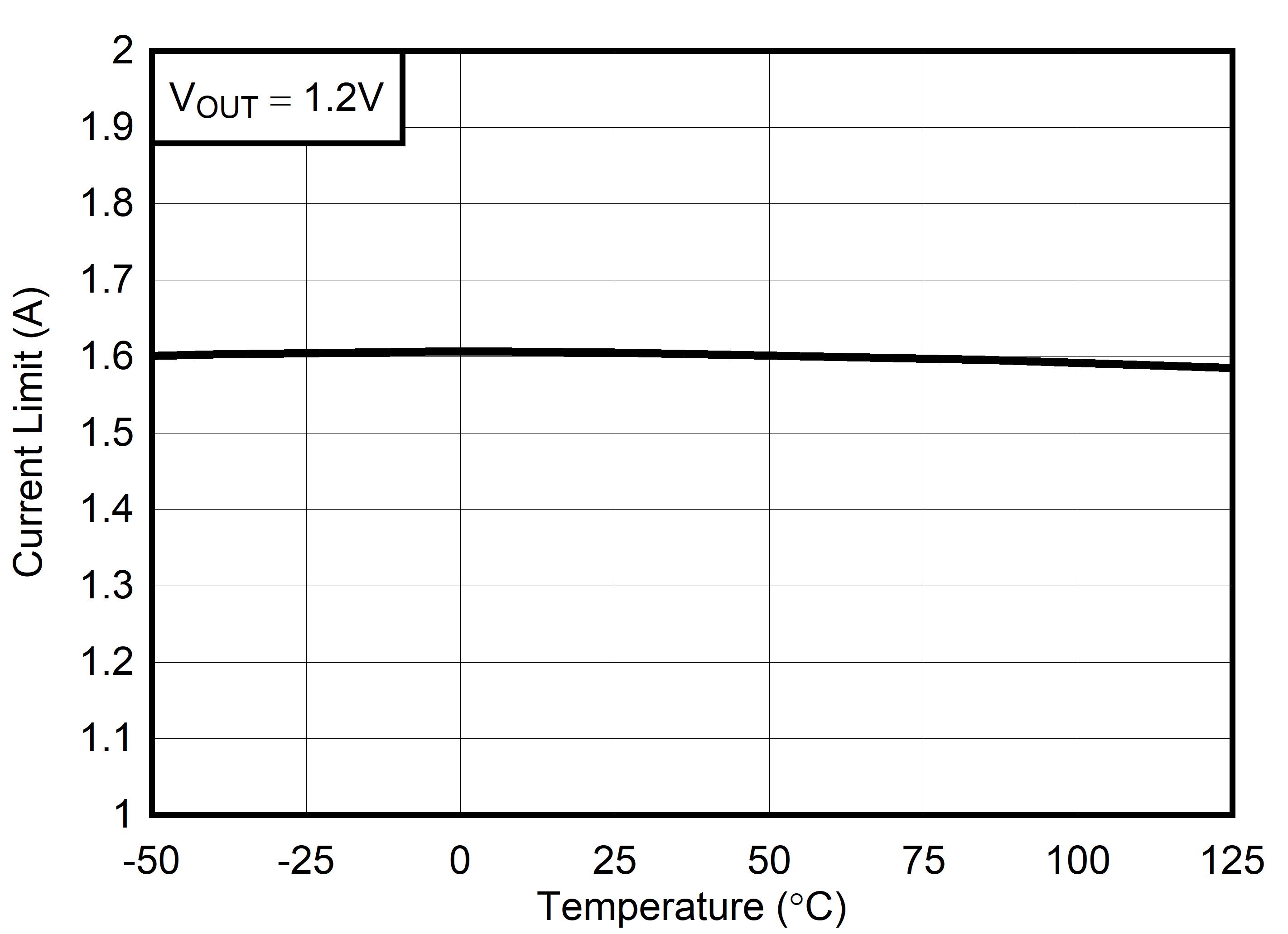
 Figure 5-21 Current Limit vs Temperature
| COUT = 1 μF, new silicon, M3 suffix |
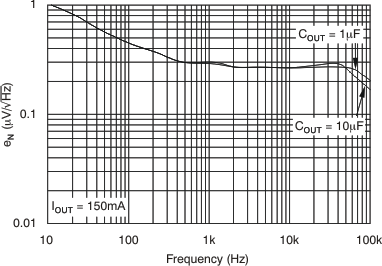
 Figure 5-25 Noise Spectral Density
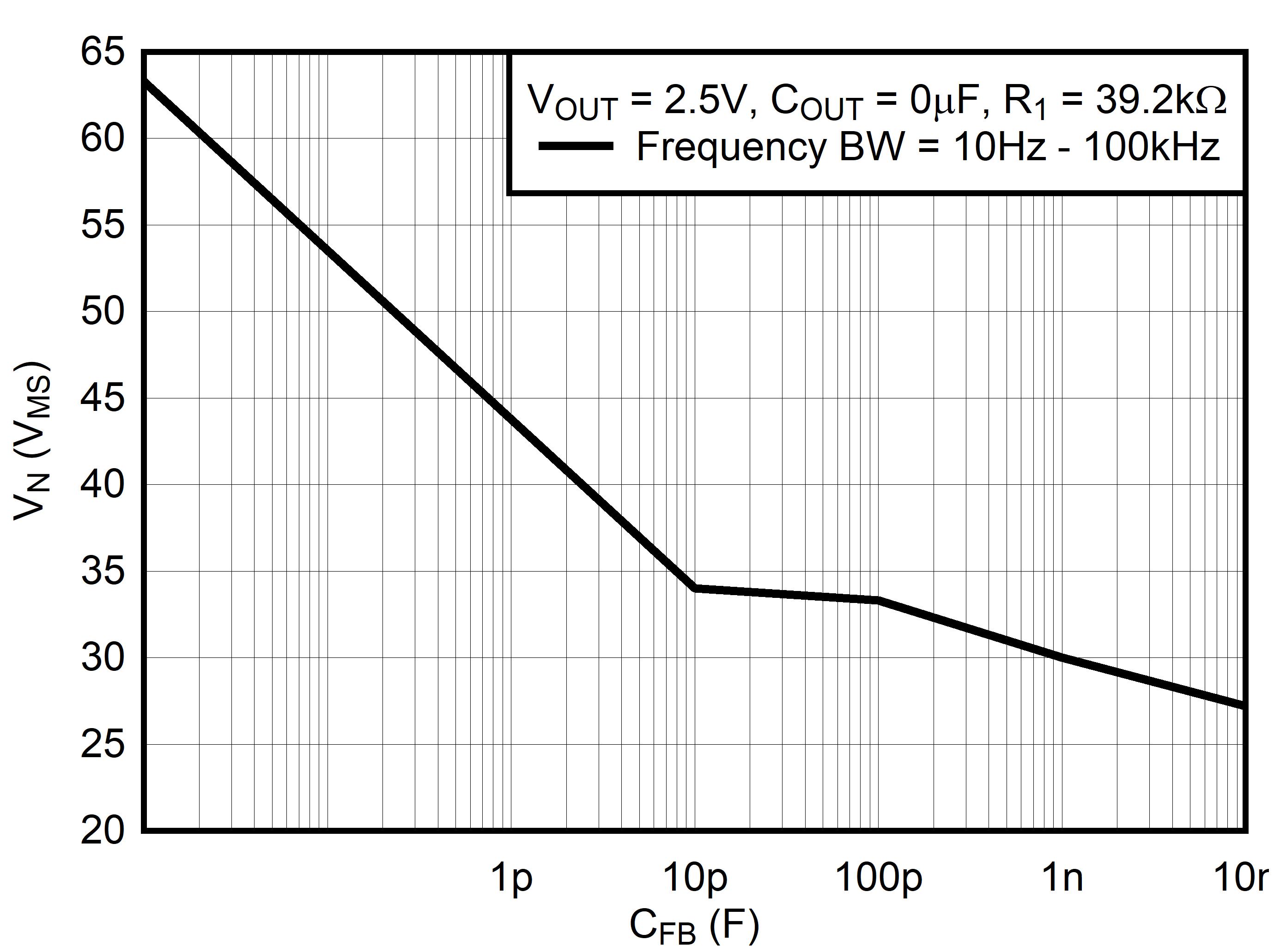
 Figure 5-27 TPS73701 RMS Noise Voltage vs CFB
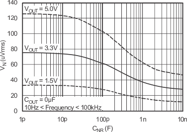
 Figure 5-29 RMS Noise Voltage vs CNR
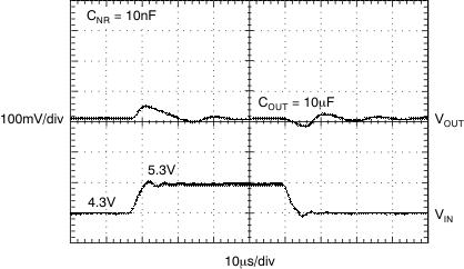
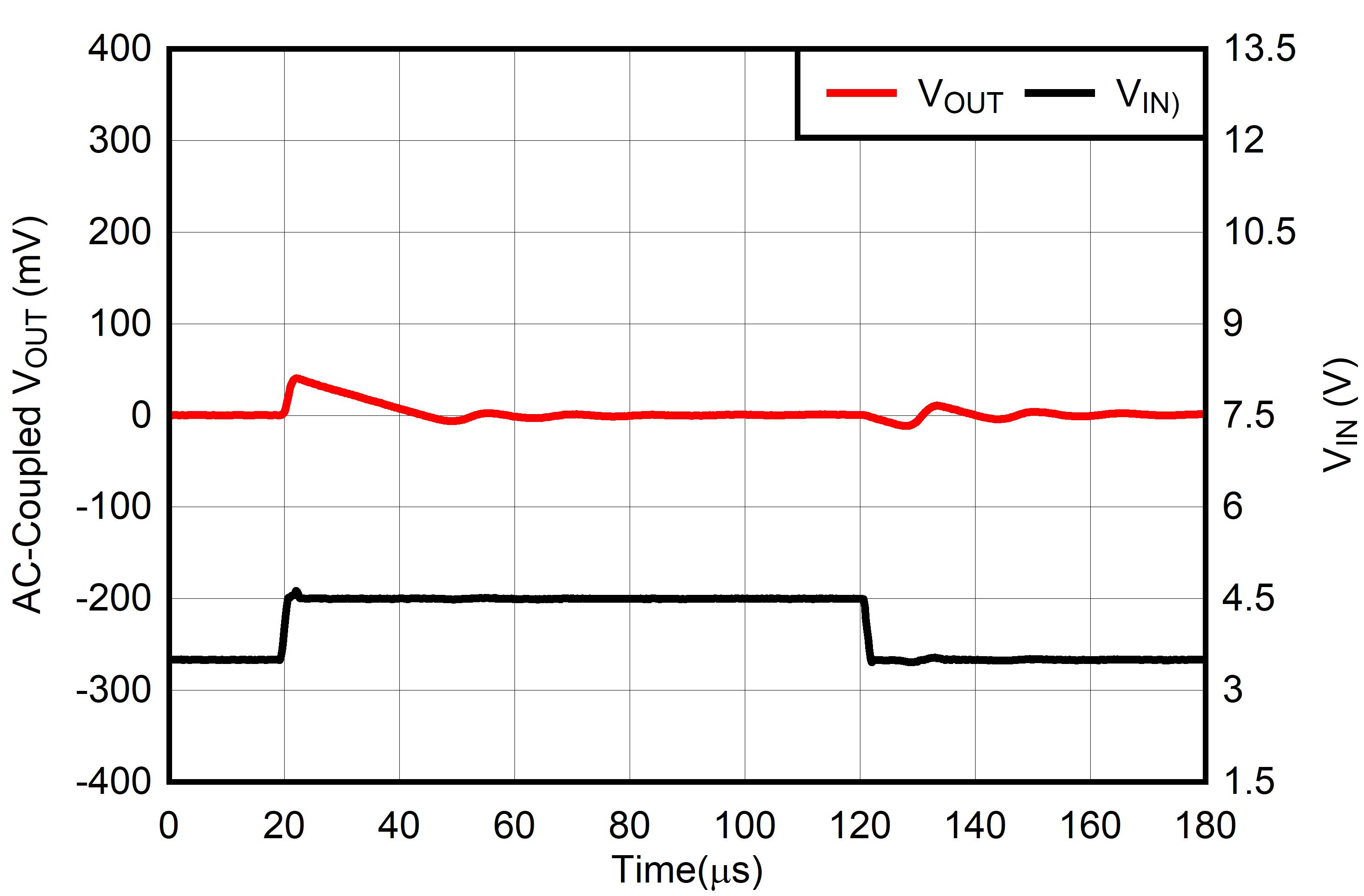
 Figure 5-31 TPS73733 Line Transient Response
 Figure 5-33 TPS73701 Turn-On Response
 Figure 5-35 TPS73701 Turn-Off Response
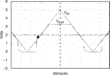
 Figure 5-37 TPS73701, VOUT = 3.3-V Power-Up and Power-Down
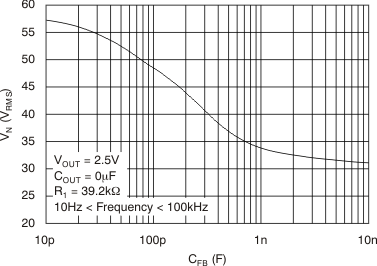
 Figure 5-39 TPS73701 RMS Noise Voltage vs CFB
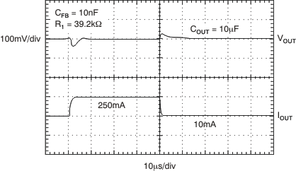
 Figure 5-41 TPS73701 Load Transient, Adjustable Version
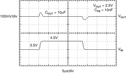
 Figure 5-43 TPS73701 Line Transient, Adjustable Version
 Figure 5-2 Load Regulation
 Figure 5-4 Line Regulation
 Figure 5-6 Dropout Voltage vs Output Current
 Figure 5-8 Dropout Voltage vs Temperature
 Figure 5-10 Output Voltage Drift Histogram
 Figure 5-12 Ground Pin Current vs Output Current
 Figure 5-14 Ground Pin Current vs Temperature
 Figure 5-16 Ground Pin Current in Shutdown vs Temperature
 Figure 5-18 Current Limit vs VIN
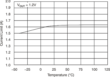
 Figure 5-20 Current Limit vs Temperature
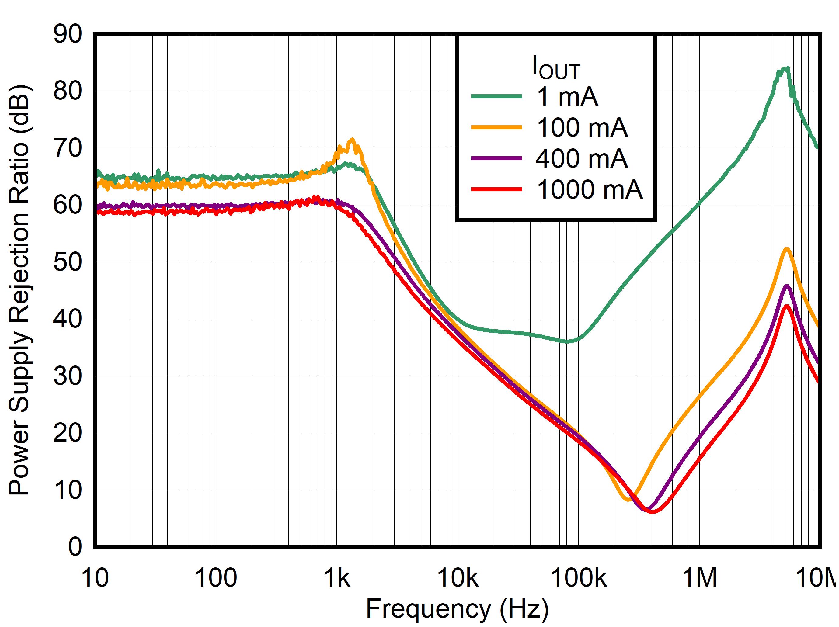
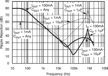
 Figure 5-22 PSRR (Ripple Rejection) vs Frequency
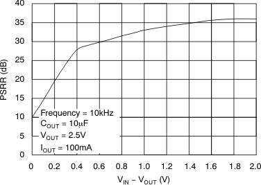
 Figure 5-24 PSRR (Ripple Rejection) vs (VIN – VOUT)
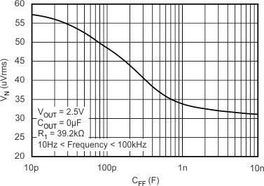
 Figure 5-26 TPS73701 RMS Noise Voltage vs CFB
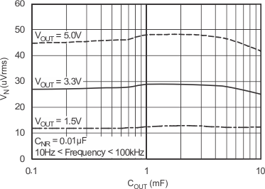
 Figure 5-28 RMS Noise Voltage vs COUT
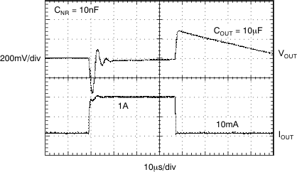
 Figure 5-30 TPS73733 Load Transient Response
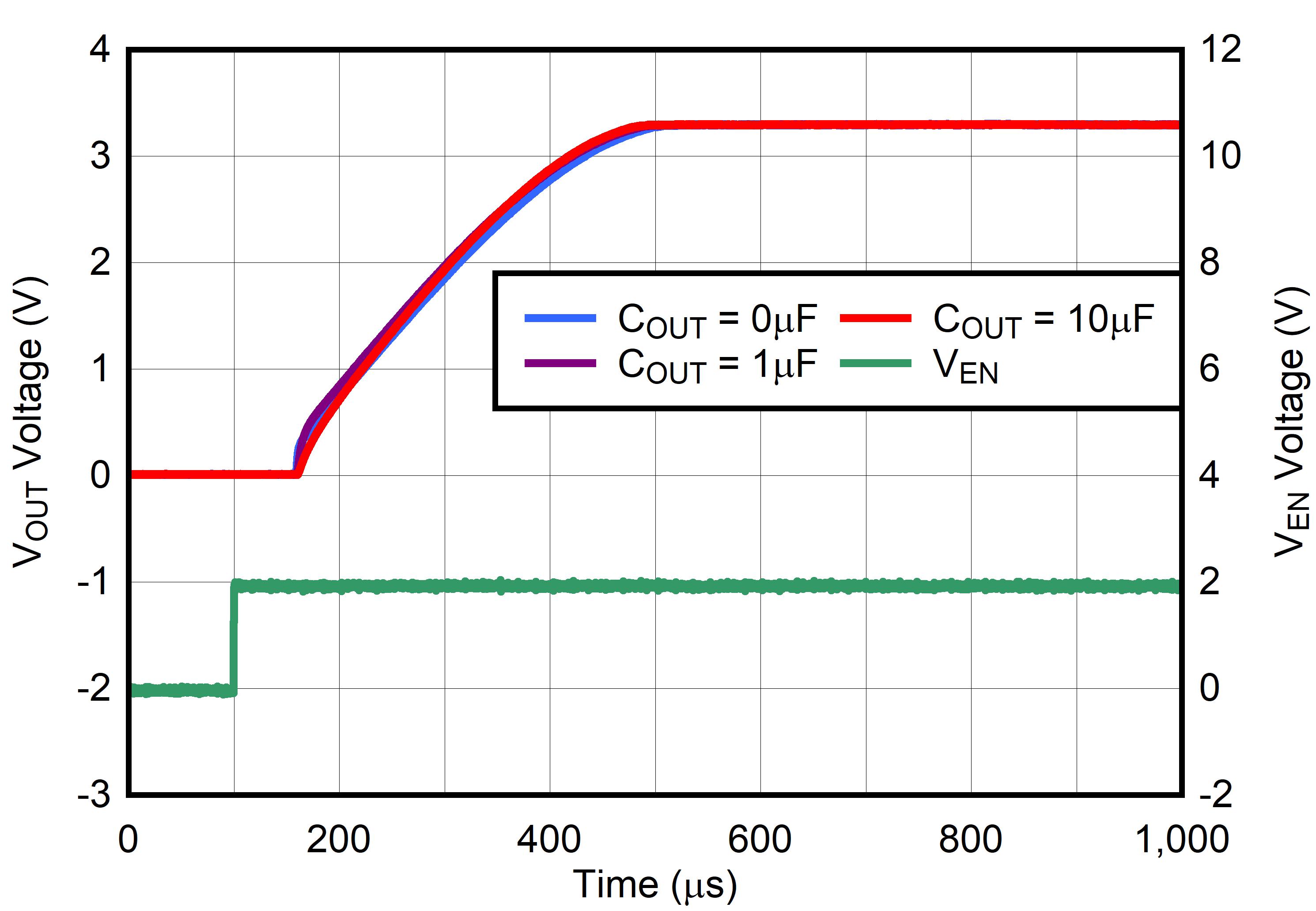
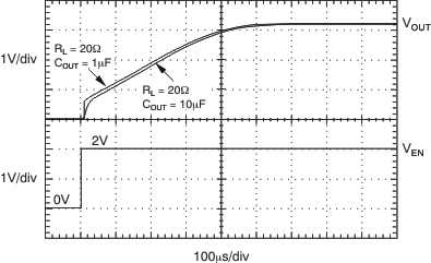
 Figure 5-32 TPS73701 Turn-On Response
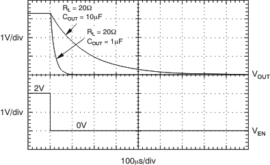
 Figure 5-34 TPS73701 Turn-Off Response
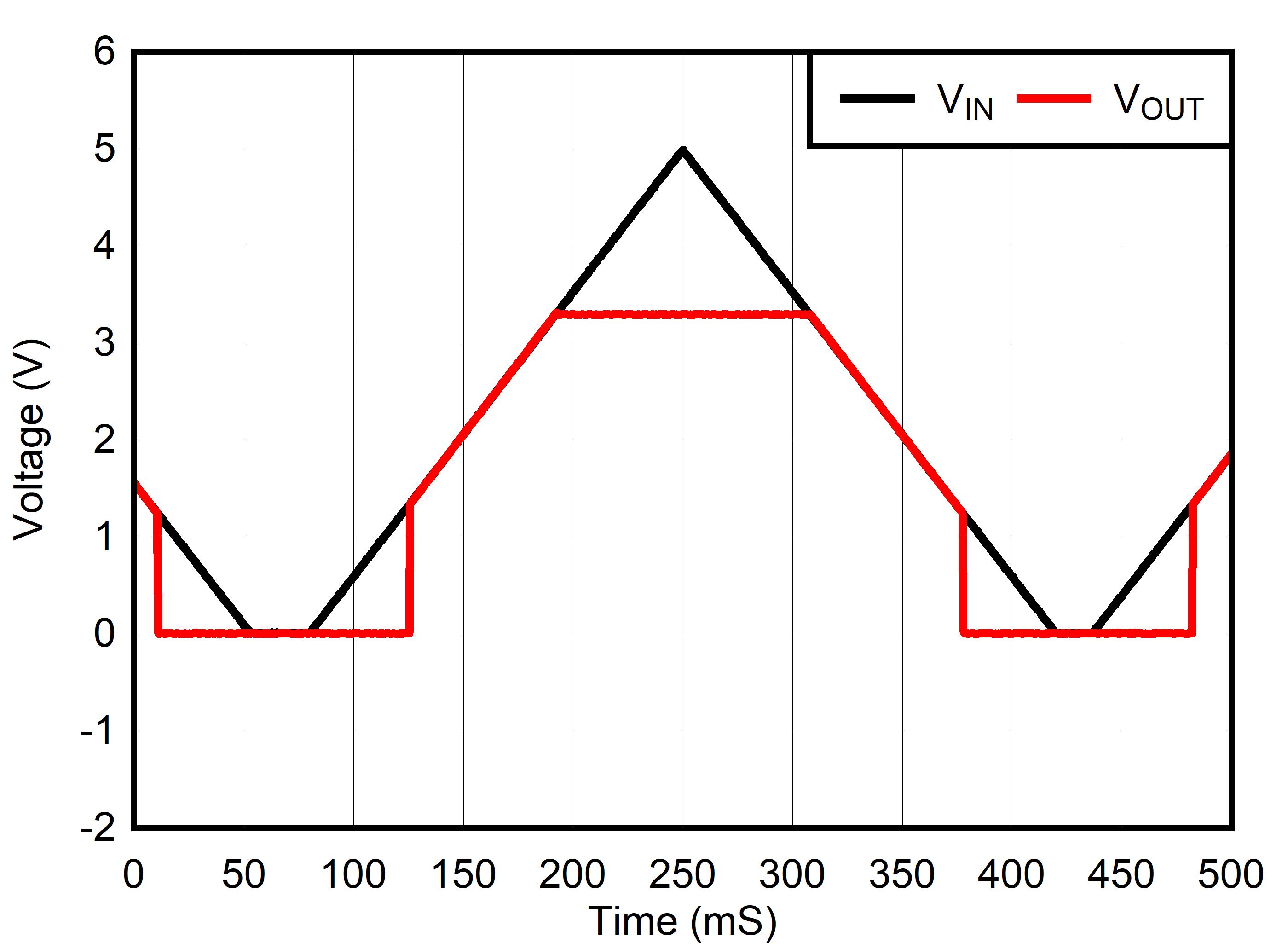
 Figure 5-36 TPS73701, VOUT = 3.3-V Power-Up and Power-Down
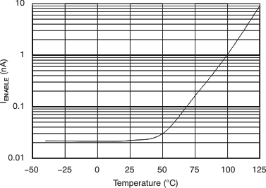
 Figure 5-38 IEN vs Temperature
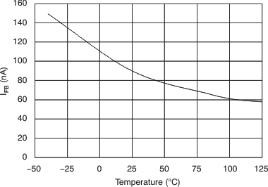
 Figure 5-40 TPS73701 IFB vs Temperature
 Figure 5-42 TPS73701 Line Transient, Adjustable Version