SBVS141D April   2010  – December 2023 TPS74701-Q1

PRODUCTION DATA  

  1.   1
  2. Features
  3. Applications
  4. Description
  5. Pin Configuration and Functions
  6. Specifications
    1. 5.1 Absolute Maximum Ratings
    2. 5.2 ESD Ratings
    3. 5.3 Recommended Operating Conditions
    4. 5.4 Thermal Information
    5. 5.5 Electrical Characteristics
    6. 5.6 Typical Characteristics: IOUT = 50 mA
    7. 5.7 Typical Characteristics: VEN = VIN = 1.8 V, VOUT = 1.5 V
  7. Detailed Description
    1. 6.1 Overview
    2. 6.2 Functional Block Diagram
    3. 6.3 Feature Description
      1. 6.3.1 Transient Response
      2. 6.3.2 Dropout Voltage
      3. 6.3.3 Output Noise
      4. 6.3.4 Enable and Shutdown
      5. 6.3.5 Power Good
      6. 6.3.6 Internal Current Limit
      7. 6.3.7 Thermal Protection
    4. 6.4 Device Functional Modes
      1. 6.4.1 Normal Operation
      2. 6.4.2 Dropout Operation
      3. 6.4.3 Disabled
  8. Application and Implementation
    1. 7.1 Application Information
    2. 7.2 Typical Application
      1. 7.2.1 Design Requirements
      2. 7.2.2 Detailed Design Procedure
        1. 7.2.2.1 Input, Output, and Bias Capacitor Requirements
        2. 7.2.2.2 Programmable Soft-Start
        3. 7.2.2.3 Sequencing Requirements
      3. 7.2.3 Application Curves
    3. 7.3 Power Supply Recommendations
    4. 7.4 Layout
      1. 7.4.1 Layout Guidelines
        1. 7.4.1.1 Layout Recommendations and Power Dissipation
        2. 7.4.1.2 Estimating Junction Temperature
      2. 7.4.2 Layout Example
  9. Device and Documentation Support
    1. 8.1 Device Support
      1. 8.1.1 Development Support
      2. 8.1.2 Device Nomenclature
    2. 8.2 Receiving Notification of Documentation Updates
    3. 8.3 Support Resources
    4. 8.4 Trademarks
    5. 8.5 Electrostatic Discharge Caution
    6. 8.6 Glossary
  10. Revision History
  11. 10Mechanical, Packaging, and Orderable Information

Package Options

Mechanical Data (Package|Pins)
Thermal pad, mechanical data (Package|Pins)
Orderable Information

Typical Application

Figure 7-1 shows the typical application circuit for the TPS74701-Q1 adjustable output device.
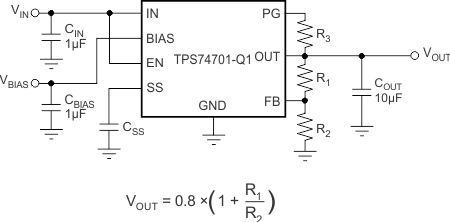
GUID-8F8E5BB4-9EAC-44B7-BCAD-C4B6D3536A12-low.gifFigure 7-1 Typical Application Circuit for the TPS74701-Q1

R1 and R2 can be calculated for any output voltage using the formula shown in Figure 7-1. See Table 7-2 for sample resistor values of common output voltages. To achieve the maximum accuracy specifications, R2 must be less than or equal to 4.99 kΩ.