SBVS141D April   2010  – December 2023 TPS74701-Q1

PRODUCTION DATA  

  1.   1
  2. Features
  3. Applications
  4. Description
  5. Pin Configuration and Functions
  6. Specifications
    1. 5.1 Absolute Maximum Ratings
    2. 5.2 ESD Ratings
    3. 5.3 Recommended Operating Conditions
    4. 5.4 Thermal Information
    5. 5.5 Electrical Characteristics
    6. 5.6 Typical Characteristics: IOUT = 50 mA
    7. 5.7 Typical Characteristics: VEN = VIN = 1.8 V, VOUT = 1.5 V
  7. Detailed Description
    1. 6.1 Overview
    2. 6.2 Functional Block Diagram
    3. 6.3 Feature Description
      1. 6.3.1 Transient Response
      2. 6.3.2 Dropout Voltage
      3. 6.3.3 Output Noise
      4. 6.3.4 Enable and Shutdown
      5. 6.3.5 Power Good
      6. 6.3.6 Internal Current Limit
      7. 6.3.7 Thermal Protection
    4. 6.4 Device Functional Modes
      1. 6.4.1 Normal Operation
      2. 6.4.2 Dropout Operation
      3. 6.4.3 Disabled
  8. Application and Implementation
    1. 7.1 Application Information
    2. 7.2 Typical Application
      1. 7.2.1 Design Requirements
      2. 7.2.2 Detailed Design Procedure
        1. 7.2.2.1 Input, Output, and Bias Capacitor Requirements
        2. 7.2.2.2 Programmable Soft-Start
        3. 7.2.2.3 Sequencing Requirements
      3. 7.2.3 Application Curves
    3. 7.3 Power Supply Recommendations
    4. 7.4 Layout
      1. 7.4.1 Layout Guidelines
        1. 7.4.1.1 Layout Recommendations and Power Dissipation
        2. 7.4.1.2 Estimating Junction Temperature
      2. 7.4.2 Layout Example
  9. Device and Documentation Support
    1. 8.1 Device Support
      1. 8.1.1 Development Support
      2. 8.1.2 Device Nomenclature
    2. 8.2 Receiving Notification of Documentation Updates
    3. 8.3 Support Resources
    4. 8.4 Trademarks
    5. 8.5 Electrostatic Discharge Caution
    6. 8.6 Glossary
  10. Revision History
  11. 10Mechanical, Packaging, and Orderable Information

Package Options

Mechanical Data (Package|Pins)
Thermal pad, mechanical data (Package|Pins)
Orderable Information

Description

The TPS74701-Q1 low-dropout (LDO) linear regulator provides an easy-to-use, robust power management solution for a wide variety of applications. The user-programmable soft-start minimizes stress on the input power source by reducing capacitive inrush current and the monotonic start-up is designed for powering many different types of processors and ASICs. The enable input and power-good output allow easy sequencing with external regulators, allowing a solution to be configured that meets the sequencing requirements for a wide range of applications with special start-up requirements.

A precision reference and error amplifier deliver 0.95% accuracy over load, line, temperature, and process. The device is stable with any type of capacitor greater than or equal to 2.2 µF, and is fully specified per AEC-Q100.
Package Information
PART NUMBER PACKAGE(1) PACKAGE SIZE(2)
TPS74701-Q1 DRC (VSON, 10) 3 mm × 3 mm
For more information, see the Mechanical, Packaging, and Orderable Information.
The package size (length × width) is a nominal value and includes pins, where applicable.


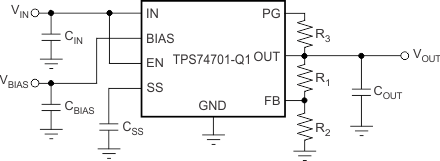
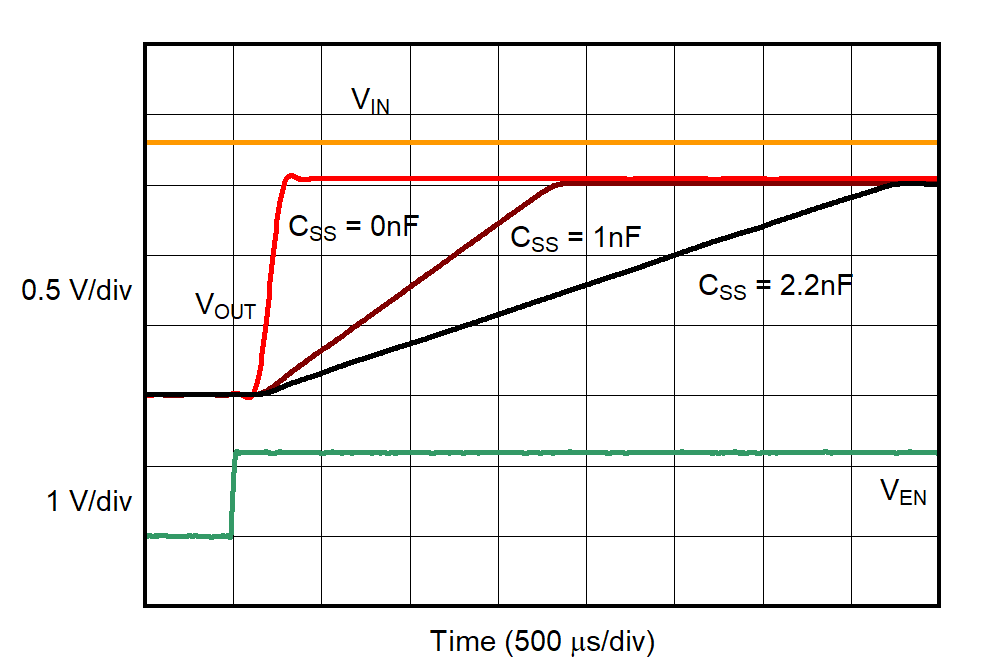
GUID-4DAFA5F5-8008-46C6-A363-9239A55F91FD-low.gifTypical Application Circuit (Adjustable)
GUID-20230410-SS0I-RQVG-P0JG-CNS6GBNKHDNJ-low.pngTurn-On Response