SBVS316B September 2018 – December 2020 TPS7A11
PRODUCTION DATA
- 1 Features
- 2 Applications
- 3 Description
- 4 Revision History
- 5 Pin Configuration and Functions
- 6 Specifications
- 7 Detailed Description
-
8 Application and Implementation
- 8.1
Application Information
- 8.1.1 Recommended Capacitor Types
- 8.1.2 Input and Output Capacitor Requirements
- 8.1.3 Load Transient Response
- 8.1.4 Dropout Voltage
- 8.1.5 Behavior During Transition From Dropout Into Regulation
- 8.1.6 Undervoltage Lockout Circuit Operation
- 8.1.7 Power Dissipation (PD)
- 8.1.8 Estimating Junction Temperature
- 8.1.9 Recommended Area for Continuous Operation
- 8.2 Typical Application
- 8.1
Application Information
- 9 Power Supply Recommendations
- 10Layout
- 11Device and Documentation Support
Package Options
Mechanical Data (Package|Pins)
Thermal pad, mechanical data (Package|Pins)
- DRV|6
Orderable Information
3 Description
The TPS7A11 is an ultra-small, low quiescent current, low-dropout regulator (LDO). This device can source 500 mA with an outstanding ac performance (load and line transient responses). This device has an input range of 0.75 V to 3.3 V, and an output range of 0.5 V to 3.0 V with a very high accuracy of 1.5% over load, line, and temperature. This performance is ideal for supplying power to the lower core voltages of modern microcontrollers (MCUs) and analog sensors.
The primary power path is through the IN pin and can be connected to a power supply as low as 140 mV above the output voltage. This device supports very low input voltages with the use of an additional VBIAS rail that is used to power the internal circuitry of the LDO. The IN and BIAS pins consume very low quiescent current of 1.6 µA and 6 µA, respectively. The low IQ and ultra-low dropout features help to increase the efficiency of the solution in power-sensitive applications. For example, the supply voltage to the IN pin can be an output of a high-efficiency, DC/DC step-down regulator and the BIAS pin supply voltage can be a rechargeable battery.
The TPS7A11 is equipped with an active pulldown circuit to quickly discharge the output when disabled, and provides a known start-up state.
The TPS7A11 is available in a small 2.00-mm × 2.00-mm WSON, 6-pin (DRV) package and an ultra-small 0.74-mm × 1.09-mm, 5-pin DSBGA (YKA) package that makes the device suitable for space-constrained applications.
| PART NUMBER | PACKAGE | BODY SIZE (NOM) |
|---|---|---|
| TPS7A11 | WSON (6) | 2.00 mm × 2.00 mm |
| DSBGA (5) | 0.74 mm × 1.09 mm (0.35-mm pitch) |
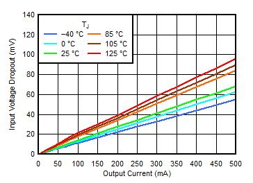
 Dropout vs IOUT and Temperature, YKA Package