SBVS136G March   2012  – October 2023 TPS7A7200

PRODUCTION DATA  

  1.   1
  2. Features
  3. Applications
  4. Description
  5. Pin Configurations
  6. Specifications
    1. 5.1 Absolute Maximum Ratings
    2. 5.2 ESD Ratings
    3. 5.3 Recommended Operating Conditions
    4. 5.4 Thermal Information
    5. 5.5 Electrical Characteristics
    6. 5.6 Typical Characteristics
  7. Detailed Description
    1. 6.1 Overview
    2. 6.2 Functional Block Diagram
    3. 6.3 Feature Description
      1. 6.3.1 User-Configurable Output Voltage
      2. 6.3.2 Traditional Adjustable Configuration
      3. 6.3.3 Undervoltage Lockout (UVLO)
      4. 6.3.4 Soft-Start
      5. 6.3.5 Current Limit
      6. 6.3.6 Enable
      7. 6.3.7 Power-Good
    4. 6.4 Device Functional Modes
      1. 6.4.1 Normal Operation
      2. 6.4.2 Dropout Operation
      3. 6.4.3 Disabled
  8. Application and Implementation
    1. 7.1 Application Information
    2. 7.2 Typical Application
      1. 7.2.1 Design Requirements
      2. 7.2.2 Detailed Design Procedure
        1. 7.2.2.1 ANY-OUT Programmable Output Voltage
        2. 7.2.2.2 Traditional Adjustable Output Voltage
        3. 7.2.2.3 Input Capacitor Requirements
        4. 7.2.2.4 Output Capacitor Requirements
      3. 7.2.3 Application Curves
    3. 7.3 Power Supply Recommendations
    4. 7.4 Layout
      1. 7.4.1 Layout Guidelines
        1. 7.4.1.1 Thermal Considerations
        2. 7.4.1.2 Power Dissipation
        3. 7.4.1.3 Estimating Junction Temperature
      2. 7.4.2 Layout Example
  9. Device And Documentation Support
    1. 8.1 Documentation Support
      1. 8.1.1 Related Documentation
    2. 8.2 Receiving Notification of Documentation Updates
    3. 8.3 Support Resources
    4. 8.4 Trademarks
    5. 8.5 Electrostatic Discharge Caution
    6. 8.6 Glossary
  10. Revision History
  11. 10Mechanical, Packaging, And Orderable Information

Package Options

Refer to the PDF data sheet for device specific package drawings

Mechanical Data (Package|Pins)
  • RGT|16
  • RGW|20
Thermal pad, mechanical data (Package|Pins)
Orderable Information

Typical Characteristics

at TJ = 25°C, VIN = VOUT(TARGET) + 0.3 V, IOUT = 25 mA, V(EN) = VIN, CIN = 10 μF, COUT = 10 μF, C(SS) = 10 nF, and the PG pin pulled up to VIN with a 100-kΩ pullup resistor (unless otherwise noted)
GUID-F9C51271-409E-4662-B160-6554200F0D69-low.png
 
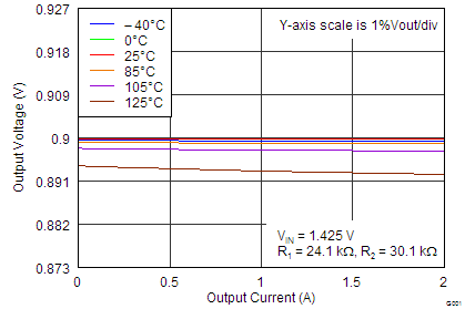
Figure 5-1 Load Regulation (0.9 V, Adjustable)
GUID-19C96C1C-7F7F-4DF9-932A-AF8E01B2DC2B-low.png
 
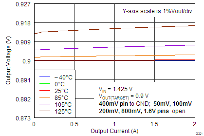
Figure 5-3 Load Regulation (0.9 V, Fixed By Setting Pins)
GUID-CE781816-2F63-4E72-A260-B9C65BF7ACA8-low.png
 
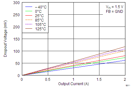
Figure 5-5 Dropout Voltage vs Output Current
GUID-ECE8447C-E1CD-466F-9D84-C805D5521506-low.png
 
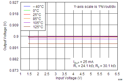
Figure 5-7 Line Regulation (0.9 V, Adjustable)
GUID-20D9BAC7-29D5-46D8-9F5B-61316EE028C0-low.png
 
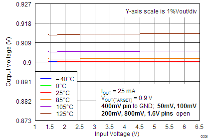
Figure 5-9 Line Regulation (0.9 V, Fixed By Setting Pins)
GUID-A68B9796-BB1D-45F4-8725-4CAA7E7155D0-low.png
 
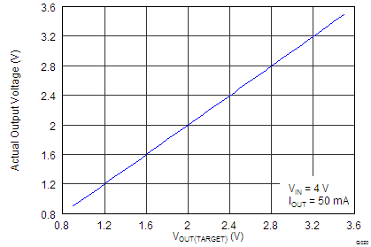
Figure 5-11 Measured Output Voltage vs Pin Setting
GUID-A98AA00B-E6BD-49CA-B7FB-485056B2AF67-low.png
 
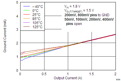
Figure 5-13 GND Pin Current vs Output Current
GUID-172CD914-298B-45D9-AE49-C3C92ECBC8F3-low.png
 
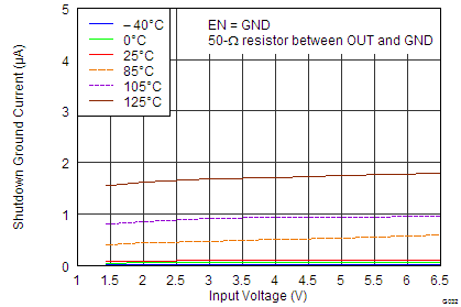
Figure 5-15 GND Pin Current In Shutdown vs Temperature
GUID-17116BEB-3AB0-49AC-873E-312E6507FB44-low.png
 
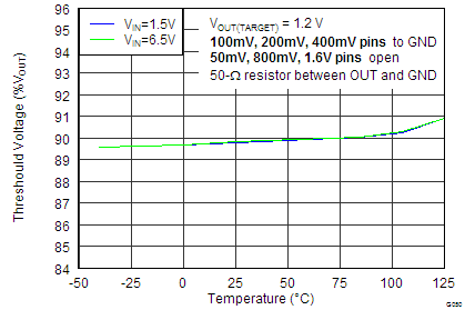
Figure 5-17 Power-Good Threshold Voltage vs Temperature
GUID-8CF7D222-E85E-400F-961C-FC1FB5310E64-low.png
 
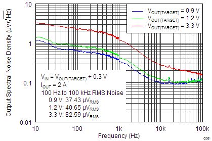
Figure 5-19 Noise Spectral Density By Output Voltage
GUID-2A96E39F-BDE4-4599-ACC6-803903CD94FC-low.png
 
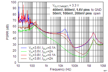
Figure 5-21 Power-Supply Ripple Rejection vs Frequency
GUID-AB4AEA69-D917-415F-A27E-CAAD52153180-low.png
 
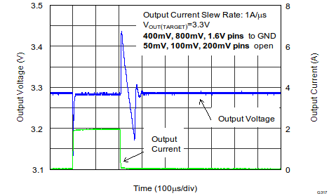
Figure 5-23 Load Transient Response (VOUT = 3.3 V)
GUID-AE370A71-1B07-4B6D-9471-6F8E55E08AB8-low.png
 
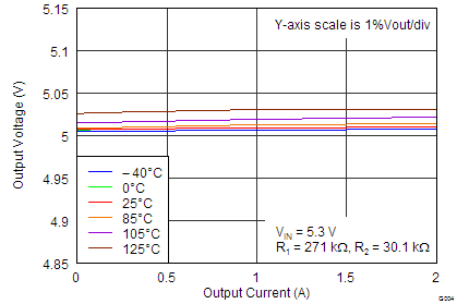
Figure 5-2 Load Regulation (5.0 V, Adjustable)
GUID-494F058D-7AB8-4DE0-AE79-138047A35DF2-low.png
 
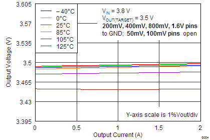
Figure 5-4 Load Regulation (3.5 V, Fixed By Setting Pins)
GUID-BBB24F66-8FEE-456D-917E-A8CD47BB3CED-low.png
 
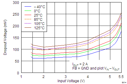
Figure 5-6 Dropout Voltage vs Temperature
GUID-8DFB31BA-0B77-4475-9768-E086377B31DB-low.png
 
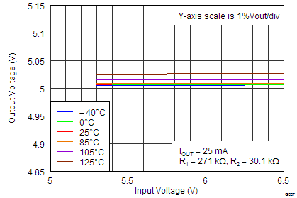
Figure 5-8 Line Regulation (5 V, Adjustable)
GUID-F2EBE96C-600F-4630-85E1-A85FC0B221B2-low.png
 
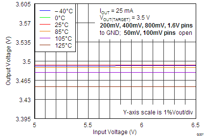
Figure 5-10 Line Regulation (3.5 V, Fixed By Setting Pins)
GUID-64F5081F-EBFC-4938-BED1-9E466D06DA6F-low.png
 
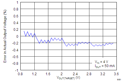
Figure 5-12 Accuracy vs Pin Setting
GUID-2252A9C5-20BC-4B90-919E-14D922732D02-low.png
 
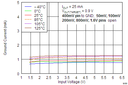
Figure 5-14 GND Pin Current vs Input Voltage
GUID-90A3AA13-4FCC-4DEB-8503-F8100F2D34BF-low.png
 
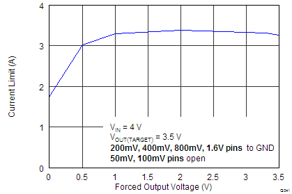
Figure 5-16 Current Limit vs Output Voltage (Foldback)
GUID-B9B8DC95-AB4A-4F53-83DC-424174019542-low.png
 
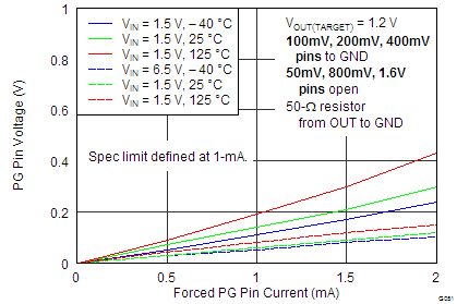
Figure 5-18 Power-Good Pin Drive Capability
GUID-28533646-306C-4B14-9886-AF6098C0C5EB-low.png
 
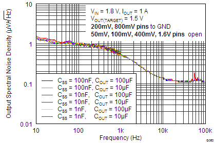
Figure 5-20 Noise Spectral Density By External Capacitors
GUID-4C78B809-9222-4536-B62B-E90993C32EB0-low.png
 
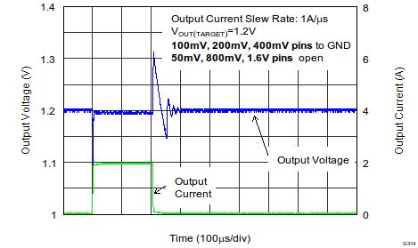
Figure 5-22 Load Transient Response (VOUT = 1.2 V)