SBVS136G March 2012 – October 2023 TPS7A7200
PRODUCTION DATA
- 1
- 1 Features
- 2 Applications
- 3 Description
- 4 Pin Configurations
- 5 Specifications
- 6 Detailed Description
- 7 Application and Implementation
- 8 Device And Documentation Support
- 9 Revision History
- 10Mechanical, Packaging, And Orderable Information
Package Options
Refer to the PDF data sheet for device specific package drawings
Mechanical Data (Package|Pins)
- RGT|16
- RGW|20
Thermal pad, mechanical data (Package|Pins)
Orderable Information
7.4.1.2 Power Dissipation
Knowing the device power dissipation and proper sizing of the thermal plane that is connected to the tab or pad is critical to avoiding thermal shutdown and providing reliable operation.
Power dissipation of the device depends on input voltage and load conditions and can be calculated using Equation 1:
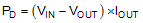
Power dissipation can be minimized and greater efficiency can be achieved by using the lowest possible input voltage necessary to achieve the required output voltage regulation.
On the VQFN (RGW or RGT) package, the primary conduction path for heat is through the exposed pad to the PCB. The pad can be connected to ground or be left floating; however, the pad must be attached to an appropriate amount of copper PCB area to make sure the device does not overheat. The maximum junction-to-ambient thermal resistance depends on the maximum ambient temperature, maximum device junction temperature, and power dissipation of the device and can be calculated using Equation 2:
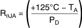
Knowing the maximum RθJA, the minimum amount of PCB copper area needed for appropriate heat sinking can be estimated using Figure 7-13.
 Figure 7-13 RθJA vs Board Size
Figure 7-13 shows the variation of RθJA as a function of ground plane copper area in the board. This figure is intended only as a guideline to demonstrate the effects of heat spreading in the ground plane and must not be used to estimate actual thermal performance in real application environments.
When the device is mounted on an application PCB, ΨJT and ΨJB must be used as explained in the Estimating Junction Temperature section.