SLVSE06B January   2018  – JANUARY 2019 TPSM846C24

PRODUCTION DATA.  

  1. Features
  2. Applications
  3. Description
    1.     Device Images
      1.      Simplified Schematic
      2.      Efficiency vs Output Current
  4. Revision History
  5. Pin Configuration and Functions
    1.     Pin Functions
  6. Specifications
    1. 6.1 Absolute Maximum Ratings
    2. 6.2 ESD Ratings
    3. 6.3 Recommended Operating Conditions
    4. 6.4 Thermal Information
    5. 6.5 Electrical Characteristics
    6. 6.6 Switching Characteristics
    7. 6.7 Typical Characteristics (VIN = 12 V)
    8. 6.8 Typical Characteristics (VIN = 5 V)
  7. Detailed Description
    1. 7.1 Overview
    2. 7.2 Functional Block Diagram
    3. 7.3 Feature Description
      1. 7.3.1  Minimum Capacitance Requirements
      2. 7.3.2  Setting the Compensation Network
      3. 7.3.3  Transient Response
      4. 7.3.4  Setting the Output Voltage
      5. 7.3.5  Differential Remote Sense
      6. 7.3.6  Switching Frequency and Synchronization
        1. 7.3.6.1 Setting the Switching Frequency
        2. 7.3.6.2 Synchronization
          1. 7.3.6.2.1 Stand-Alone Device Synchronization
          2. 7.3.6.2.2 Paralleled Devices Synchronization
      7. 7.3.7  Prebiased Output Start-Up
      8. 7.3.8  Power-Good (PGOOD) Indicator
      9. 7.3.9  Linear Regulators BP3 and BP6
      10. 7.3.10 Parallel Application
      11. 7.3.11 Parallel Operation
      12. 7.3.12 Overtemperature Protection
      13. 7.3.13 Overcurrent Protection
      14. 7.3.14 Output Overvoltage and Undervoltage Protection
    4. 7.4 Device Functional Modes
      1. 7.4.1 Active Mode
      2. 7.4.2 Shutdown Mode
  8. Application and Implementation
    1. 8.1 Typical Application
      1. 8.1.1 Design Requirements
      2. 8.1.2 Detailed Design Procedure
        1. 8.1.2.1 Custom Design With WEBENCH® Tools
        2. 8.1.2.2 Setting the Output Voltage
        3. 8.1.2.3 Input and Output Capacitance
        4. 8.1.2.4 Selecting the Compensation Components
        5. 8.1.2.5 Setting the Switching Frequency
        6. 8.1.2.6 Power Good (PGOOD)
        7. 8.1.2.7 ON/OFF Control (EN)
      3. 8.1.3 Application Curves
  9. Power Supply Recommendations
  10. 10Layout
    1. 10.1 Layout Guidelines
    2. 10.2 Layout Example
    3. 10.3 Package Specifications
    4. 10.4 EMI
    5. 10.5 Mounting and Thermal Profile Recommendation
  11. 11Device and Documentation Support
    1. 11.1 Device Support
      1. 11.1.1 Development Support
        1. 11.1.1.1 Custom Design With WEBENCH® Tools
    2. 11.2 Receiving Notification of Documentation Updates
    3. 11.3 Community Resources
    4. 11.4 Trademarks
    5. 11.5 Electrostatic Discharge Caution
    6. 11.6 Glossary
  12. 12Mechanical, Packaging, and Orderable Information
    1. 12.1 Tape and Reel Information

Package Options

Mechanical Data (Package|Pins)
Thermal pad, mechanical data (Package|Pins)
Orderable Information

EMI

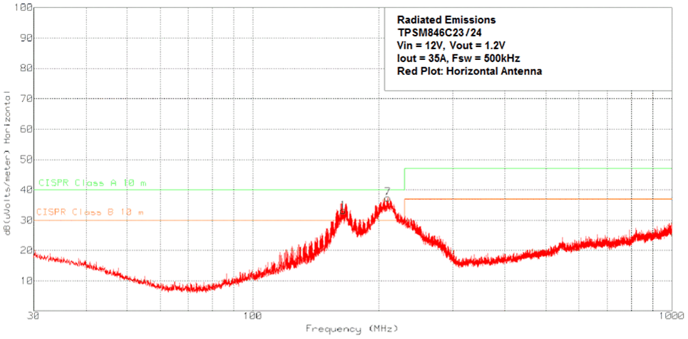
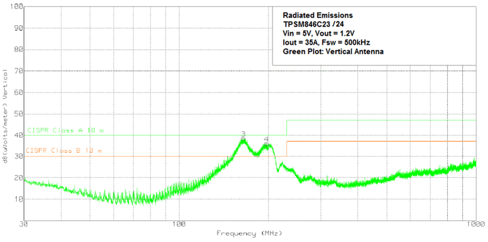
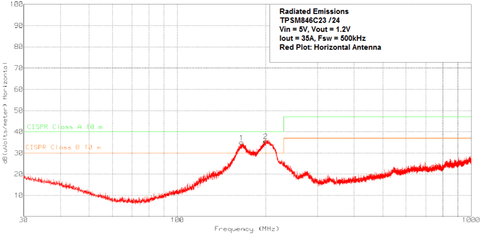
The TPSM846C24 is compliant with EN55022 Class A radiated emissions. Figure 22 to Figure 25 show typical examples of radiated emissions plots for the TPSM846C24. The EMI plots were taken using an EVM with a resistive load and input power was provided using a lead acid battery. All graphs show plots of the antenna in the horizontal and vertical positions.
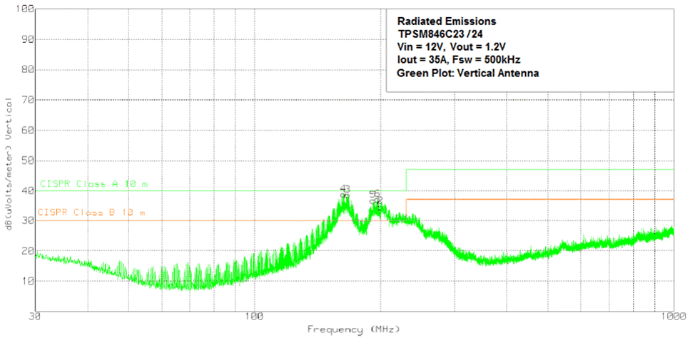
TPSM846C24 EMI12VVert.gif
Figure 22. Radiated Emissions 12-V Input, 1.2-V Output,
35-A Load Vertical Antenna
TPSM846C24 EMI12VHoriz.gif
Figure 23. Radiated Emissions 12-V Input, 1.2-V Output,
35-A Load Horizontal Antenna
TPSM846C24 EMI5VVert.gifFigure 24. Radiated Emissions 5-V Input, 1.2-V Output,
35-A Load Vertical Antenna
TPSM846C24 EMI5VHoriz.gifFigure 25. Radiated Emissions 5-V Input, 1.2-V Output,
35-A Load Horizontal Antenna