SLVSE06B January 2018 – JANUARY 2019 TPSM846C24
PRODUCTION DATA.
- 1 Features
- 2 Applications
- 3 Description
- 4 Revision History
- 5 Pin Configuration and Functions
- 6 Specifications
-
7 Detailed Description
- 7.1 Overview
- 7.2 Functional Block Diagram
- 7.3
Feature Description
- 7.3.1 Minimum Capacitance Requirements
- 7.3.2 Setting the Compensation Network
- 7.3.3 Transient Response
- 7.3.4 Setting the Output Voltage
- 7.3.5 Differential Remote Sense
- 7.3.6 Switching Frequency and Synchronization
- 7.3.7 Prebiased Output Start-Up
- 7.3.8 Power-Good (PGOOD) Indicator
- 7.3.9 Linear Regulators BP3 and BP6
- 7.3.10 Parallel Application
- 7.3.11 Parallel Operation
- 7.3.12 Overtemperature Protection
- 7.3.13 Overcurrent Protection
- 7.3.14 Output Overvoltage and Undervoltage Protection
- 7.4 Device Functional Modes
- 8 Application and Implementation
- 9 Power Supply Recommendations
- 10Layout
- 11Device and Documentation Support
- 12Mechanical, Packaging, and Orderable Information
Package Options
Mechanical Data (Package|Pins)
- MOL|59
Thermal pad, mechanical data (Package|Pins)
Orderable Information
7.3.4 Setting the Output Voltage
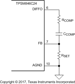
The TPSM846C24 output voltage adjustment range is 0.5 V to 2 V. The adjustment method requires a resistor, RSET, connected between the FB pin and AGND as shown in Figure 15. Equation 1 can be used to calculate the RSET value for a given output voltage, VOUT. Additionally, the RSET value can be selected from Table 3.
 Figure 15. RSET Resistor
 Equation 1. 

Table 3. Standard RSET Resistor Values
| VOUT (V) | RSET (kΩ) | VOUT (V) | RSET (kΩ) | |
|---|---|---|---|---|
| 0.5 | open | 1.3 | 6.19 | |
| 0.6 | 49.9 | 1.4 | 5.49 | |
| 0.7 | 24.9 | 1.5 | 4.99 | |
| 0.8 | 16.5 | 1.6 | 4.53 | |
| 0.9 | 12.4 | 1.7 | 4.12 | |
| 1 | 10 | 1.8 | 3.83 | |
| 1.1 | 8.25 | 1.9 | 3.57 | |
| 1.2 | 7.15 | 2.0 | 3.32 |