SLWS245B May 2014 – February 2017 TRF3722
PRODUCTION DATA.
- 1 Features
- 2 Applications
- 3 Description
- 4 Revision History
- 5 Pin Configuration and Functions
-
6 Specifications
- 6.1 Absolute Maximum Ratings
- 6.2 ESD Ratings
- 6.3 Recommended Operating Conditions
- 6.4 Thermal Information
- 6.5 Electrical Characteristics
- 6.6 Typical Characteristics
- 6.7 Typical Characteristics - Output Power
- 6.8 Typical Characteristics - Gain
- 6.9 Typical Characteristics - OIP3
- 6.10 Typical Characteristics - OIP2
- 6.11 Typical Characteristics - OP1dB
- 6.12 Typical Characteristics - Noise
- 6.13 Typical Characteristics - Unadjusted CF
- 6.14 Typical Characteristics - Unadjusted SBS
- 6.15 Typical Characteristics - LO Harmonic
- 6.16 Typical Characteristics - BB Harmonic
- 6.17 Typical Characteristics - RF Output Return Loss
- 6.18 Typical Characteristics - PLL/VCO
- 6.19 Typical Characteristics - Current Consumption
- 6.20 Typical Characteristics - Power Dissipation
- 7 Parameter Measurement Information
- 8 Detailed Description
- 9 Application and Implementation
- 10Power Supply Recommendations
- 11Layout
- 12Device and Documentation Support
- 13Mechanical, Packaging, and Orderable Information
Package Options
Mechanical Data (Package|Pins)
- RGZ|48
Thermal pad, mechanical data (Package|Pins)
- RGZ|48
Orderable Information
6 Specifications
6.1 Absolute Maximum Ratings
over operating free-air temperature range (unless otherwise noted)(1)| MIN | MAX | UNIT | ||
|---|---|---|---|---|
| Supply voltage | All VCC except VCC_TK | –0.3 | +3.6 | V |
| VCC_TK | –0.3 | +5.5 | ||
| Digital I/O voltage | –0.3 | 3.6 | V | |
| Operating junction temperature | –40 | 150 | °C | |
| Storage temperature, Tstg | –40 | 150 | °C | |
(1) Stresses beyond those listed under Absolute Maximum Ratings may cause permanent damage to the device. These are stress ratings only, which do not imply functional operation of the device at these or any other conditions beyond those indicated under Recommended Operating Conditions. Exposure to absolute-maximum-rated conditions for extended periods may affect device reliability.
6.2 ESD Ratings
| VALUE | UNIT | |||
|---|---|---|---|---|
| V(ESD) | Electrostatic discharge | Human-body model (HBM), per ANSI/ESDA/JEDEC JS-001(1) | ±2000 | V |
| Charged-device model (CDM), per JEDEC specification JESD22-C101(2) | ±750 | |||
(1) JEDEC document JEP155 states that 500-V HBM allows safe manufacturing with a standard ESD control process.
(2) JEDEC document JEP157 states that 250-V CDM allows safe manufacturing with a standard ESD control process.
6.3 Recommended Operating Conditions
over operating free-air temperature range (unless otherwise noted)| MIN | NOM | MAX | UNIT | ||
|---|---|---|---|---|---|
| VCC | 3.3 V power-supply voltage | 3 | 3.3 | 3.6 | V |
| 5 V or 3.3 V power-supply voltage, VCC _TK | 3 | 3.3/5 | 5.5 | V | |
| TJ | Operating junction temperature range | –40 | 125 | °C | |
| TA | Ambient temperature range | –40 | 85 | °C | |
6.4 Thermal Information
| THERMAL METRIC(1) | TRF3722 | UNIT | |
|---|---|---|---|
| RGZ (VQFN) | |||
| 48 PINS | |||
| RθJA | Junction-to-ambient thermal resistance | 27.5 | °C/W |
| RθJC(top) | Junction-to-case (top) thermal resistance | 12.8 | °C/W |
| RθJB | Junction-to-board thermal resistance | 4.3 | °C/W |
| ψJT | Junction-to-top characterization parameter | 0.2 | °C/W |
| ψJB | Junction-to-board characterization parameter | 4.3 | °C/W |
| RθJC(bot) | Junction-to-case (bottom) thermal resistance | 0.8 | °C/W |
(1) For more information about traditional and new thermal metrics, see the Semiconductor and IC Package Thermal Metrics application report.
6.5 Electrical Characteristics
Over recommended operating conditions: VCC = 3.3 V, VCC_TK = 5 V, TA = 25°C. Optimized bias settings as per Table 16.| PARAMETER | TEST CONDITIONS | MIN | TYP | MAX | UNIT | |
|---|---|---|---|---|---|---|
| DC PARAMETERS | ||||||
| ICC | 3.3 V Supply Current | Typical Operating Mode; LO out = Off | 328(1) | mA | ||
| Typical Operating Mode; LO out = On | 374 | mA | ||||
| ICC_TK | 5 V Supply Current | 21 | mA | |||
| PDISS | Total Power Dissipation | Typical Operating Mode; LO out = Off | 1.18 | W | ||
| Typical Operating Mode; LO out = On | 1.34 | W | ||||
| Low Power Mode (Mod); LO out = Off | 0.91 | W | ||||
| IPD | Power Down Current | Hardware Power Down | 76 | mA | ||
| Serial interface Power Down | 2 | mA | ||||
| RFOUT FREQUENCY | ||||||
| Frequency | 400 | 4200 | MHz | |||
| IQ MODULATOR ƒLO = 750 MHz | ||||||
| G | Gain | Typical Operating Mode | 0.8 | dB | ||
| High Gain Mode | 3.6 | dB | ||||
| Gain Flatness | In 300MHz bandwidth | –0.5 | 0.5 | dB | ||
| OP1dB | Output Compression Point | 10.2 | dBm | |||
| OIP3 | Output 3rd Order Intercept Point | FBB = 4.5, 5.5 MHz | 31 | dBm | ||
| OIP2 | Output 2nd Order Intercept Point | FBB = 4.5, 5.5 MHz | 62 | dBm | ||
| SBS | Unadj. SideBand Suppression | –42 | dBc | |||
| CF | Unadj. Carrier Feedthrough | –50 | dBm | |||
| NSDO | Output Noise Spectral Density | BB inputs terminated on 50 Ω | –159 | dBm/Hz | ||
| HD2LO | LO Second Harmonic | Measured at 2 x fLO | –49 | dBc | ||
| HD3LO | LO Third Harmonic | Measured at 3 x fLO | –47 | dBc | ||
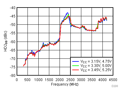
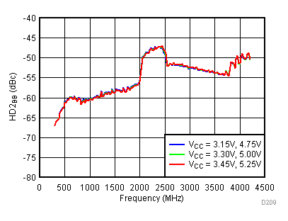
| HD2BB | Baseband Second Harmonic | Measured at fLO ± 2 x fBB | –72 | dBc | ||
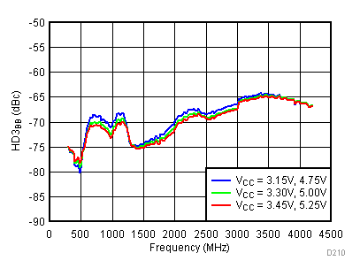
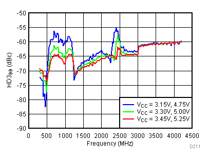
| HD3BB | Baseband Third Harmonic | Measured at fLO ± 3 x fBB | –70 | dBc | ||
| IQ MODULATOR ƒLO = 900 MHz | ||||||
| G | Gain | Typical Operating Mode | 0.8 | dB | ||
| High Gain Mode | 3.6 | dB | ||||
| Gain Flatness | In 300MHz bandwidth | –0.5 | 0.5 | dB | ||
| OP1dB | Output Compression Point | 10 | dBm | |||
| OIP3 | Output 3rd Order Intercept Point | FBB = 4.5, 5.5 MHz | 31 | dBm | ||
| OIP2 | Output 2nd Order Intercept Point | FBB = 4.5, 5.5 MHz | 62.5 | dBm | ||
| SBS | Unadj. Side Band Suppression | –42.5 | dBc | |||
| CF | Unadj. Carrier Feed through | –50 | dBm | |||
| NSDO | Output Noise Spectral Density | BB inputs terminated on 50 Ω | –159 | dBm/Hz | ||
| HD2LO | LO Second Harmonic | Measured at 2 x fLO | –47 | dBc | ||
| HD3LO | LO Third Harmonic | Measured at 3 x fLO | –54.5 | dBc | ||
| HD2BB | Baseband Second Harmonic | Measured at fLO ± 2 x fBB | –65.5 | dBc | ||
| HD3BB | Baseband Third Harmonic | Measured at fLO ± 3 x fBB | –71.5 | dBc | ||
| IQ MODULATOR ƒLO = 1800 MHz | ||||||
| G | Gain | Typical Operating Mode | 0.3 | dB | ||
| High Gain Mode | 3 | dB | ||||
| Gain Flatness | In 300 MHz bandwidth | –0.5 | 0.5 | dB | ||
| OP1dB | Output Compression Point | 13 | dBm | |||
| OIP3 | Output 3rd Order Intercept Point | fBB = 4.5, 5.5 MHz | 29.5 | dBm | ||
| OIP2 | Output 2nd Order Intercept Point | fBB = 4.5, 5.5 MHz | 57 | dBm | ||
| SBS | Unadj. Side Band Suppression | –54.5 | dBc | |||
| CF | Unadj. Carrier Feed through | –57 | dBm | |||
| NSDO | Output Noise Spectral Density | BB inputs terminated on 50 Ω | –158 | dBm/Hz | ||
| HD2LO | LO Second Harmonic | Measured at 2 x fLO | –36.5 | dBc | ||
| HD3LO | LO Third Harmonic | Measured at 3 x fLO | –33.5 | dBc | ||
| HD2BB | Baseband Second Harmonic | Measured at fLO ± 2 x fBB | –65.5 | dBc | ||
| HD3BB | Baseband Third Harmonic | Measured at fLO ± 3 x fBB | –73 | dBc | ||
| RLO | RF Output Return Loss | 6 | dB | |||
| IQ MODULATOR ƒLO = 2150 MHz | ||||||
| G | Gain | Typical Operating Mode | 0.2 | dB | ||
| High Gain Mode | 3 | dB | ||||
| Gain Flatness | In 300 MHz bandwidth | –0.5 | 0.5 | dB | ||
| OP1dB | Output Compression Point | 11.6 | dBm | |||
| OIP3 | Output 3rd Order Intercept Point | FBB = 4.5, 5.5 MHz | 30 | dBm | ||
| OIP2 | Output 2nd Order Intercept Point | FBB = 4.5, 5.5 MHz | 43 | dBm | ||
| SBS | Unadj. Side Band Suppression | –43 | dBc | |||
| CF | Unadj. Carrier Feedt hrough | –42 | dBm | |||
| NSDO | Output Noise Spectral Density | BB inputs terminated on 50 Ω | –157 | dBm/Hz | ||
| HD2LO | LO Second Harmonic | Measured at 2 x fLO | –40 | dBc | ||
| HD3LO | LO Third Harmonic | Measured at 3 x fLO | –31 | dBc | ||
| HD2BB | Baseband Second Harmonic | Measured at fLO ± 2 x fBB | –51 | dBc | ||
| HD3BB | Baseband Third Harmonic | Measured at fLO ± 3 x fBB | –69 | dBc | ||
| IQ MODULATOR ƒLO = 2700 MHz | ||||||
| G | Gain | Typical Operating Mode | 0 | dB | ||
| High Gain Mode | 2.4 | dB | ||||
| Gain Flatness | In 300MHz bandwidth | –0.5 | 0.5 | dB | ||
| OP1dB | Output Compression Point | 10.4 | dBm | |||
| OIP3 | Output 3rd Order Intercept Point | FBB = 4.5, 5.5 MHz | 29.5 | dBm | ||
| OIP2 | Output 2nd Order Intercept Point | FBB = 4.5, 5.5 MHz | 45.5 | dBm | ||
| SBS | Unadj. Side Band Suppression | –33 | dBc | |||
| CF | Unadj. Carrier Feed through | –39.6 | dBm | |||
| NSDO | Output Noise Spectral Density | BB inputs terminated on 50 Ω | –156 | dBm/Hz | ||
| HD2LO | LO Second Harmonic | Measured at 2 x fLO | –29 | dBc | ||
| HD3LO | LO Third Harmonic | Measured at 3 x fLO | –37 | dBc | ||
| HD2BB | Baseband Second Harmonic | Measured at fLO ± 2 x fBB | –53 | dBc | ||
| HD3BB | Baseband Third Harmonic | Measured at fLO ± 3 x fBB | –68 | dBc | ||
| IQ MODULATOR ƒLO = 3600 MHz | ||||||
| G | Gain | Typical Operating Mode | –2 | dB | ||
| High Gain Mode | 0.4 | dB | ||||
| OP1dB | Output Compression Point | 8.7 | dBm | |||
| OIP3 | Output 3rd Order Intercept Point | FBB = 4.5, 5.5 MHz | 24.5 | dBm | ||
| OIP2 | Output 2nd Order Intercept Point | FBB = 4.5, 5.5 MHz | 45.5 | dBm | ||
| SBS | Unadj. Side Band Suppression | –31.5 | dBc | |||
| CF | Unadj. Carrier Feed through | –39.5 | dBm | |||
| HD2LO | LO Second Harmonic | Measured at 2 x fLO | –28.4 | dBc | ||
| HD3LO | LO Third Harmonic | Measured at 3 x fLO | –31.5 | dBc | ||
| HD2BB | Baseband Second Harmonic | Measured at fLO ± 2 x fBB | –55 | dBc | ||
| HD3BB | Baseband Third Harmonic | Measured at fLO ± 3 x fBB | –65 | dBc | ||
| BASEBAND INPUTS | ||||||
| VCM | Common Mode Voltage | Baseband I/Q input | 0 | 0.25 | 0.5 | V |
| BWBB | Baseband Bandwidth | 1 dB Bandwidth | 900 | MHz | ||
| ZinBB | Baseband Input Impedance | Resistance | 5 | kΩ | ||
| Capacitance | 4 | pF | ||||
| REFERENCE OSCILLATOR PARAMETERS | ||||||
| Fref | Reference Frequency | Max | 350 | MHz | ||
| Reference Input Sensitivity | 0.2 | 3.3 | VPP | |||
| Zinref | Reference Input Impedance | Parallel capacitance | 2 | pF | ||
| Parallel resistance | 2.2 | kΩ | ||||
| PFD, CP | ||||||
| FPFD | PFD Frequency | Max, refer to the Typical Application | 65 | MHz | ||
| ICP_OUT | Charge Pump Current | Max | 1.94 | mA | ||
| In-band Normalized PN Floor | Integer Mode | –221 | dBc/Hz | |||
| VCO | ||||||
| fVCO | Typical VCO frequency range(2) | 2050 | 4100 | MHz | ||
| KV | VCO gain | VTUNE = 1.1 V | 30 | MHz/V | ||
| PN | VCO Open Loop Phase Noise; fVCO = 3600 MHz; TX Div = Div-by-1; fOUT = 3600 MHz VTUNE = 1.1 V |
10 kHz | –74 | dBc/Hz | ||
| 100 kHz | –109 | |||||
| 1 MHz | –135 | |||||
| 10 MHz | –152 | |||||
| 40 MHz | –156 | |||||
| VCO Open Loop Phase Noise; fVCO = 3600 MHz; TX Div = Div-by-2; fOUT = 1800 MHz; VTUNE = 1.1 V |
10 kHz | –80 | dBc/Hz | |||
| 100 kHz | –115 | |||||
| 1 MHz | –141 | |||||
| 10 MHz | –156 | |||||
| 40 MHz | –158 | |||||
| LO OUTPUT | ||||||
| fOUT | Typical output frequency range(2) | Divide by 1 | 2050 | 4100 | MHz | |
| Divide by 2 | 1025 | 2050 | ||||
| Divide by 4 | 512.5 | 1025 | ||||
| Divide by 8 | 256.25 | 512.5 | ||||
| PLO | Output power | SE at 1800 MHz, OUTBUF_BIAS = 2 | 1 | dBm | ||
| External VCO input Frequency Range | 250 | 4200 | MHz | |||
| External VCO Input Level | –10 | 0 | 10 | dBm | ||
| CLOSE LOOP PLL OR VCO | ||||||
| Integrated Phase Noise | Frac-N; PFD = 15.36 MHz; fOUT = 3532.89 MHz; Integration BW =1 kHz to 10 MHz; SSB |
-45.2 | dB | |||
| Int-N; PFD = 2.56 MHz; fOUT = 1799.68 MHz; Integration BW = 500 Hz to 20 MHz; SSB |
-49.8 | dB | ||||
| VCO Close Loop Phase Noise; fVCO = 3600 MHz; TX DIV = Div-by-2; fOUT = 1800 MHz; Integer Mode, PFD = 2.56MHz |
10 kHz | –96 | dBc/Hz | |||
| 100 kHz | –114 | |||||
| 1 MHz | –140 | |||||
| 10 MHz | –156 | |||||
| 40 MHz | –158 | |||||
| DIGITAL INTERFACE | ||||||
| VIH | High Level Input Voltage | 2 | 3.3 | V | ||
| VIL | Low Level Input Voltage | 0 | 0.8 | V | ||
| VOH | High Level Output Voltage | Referenced to VCC_DIG | 0.8 x VCC | V | ||
| VOL | Low Level Output Voltage | Referenced to VCC_DIG | 0.2 x VCC | V | ||
(1) Powered down output buffer and LO divider.
(2) Divided-down ranges minimum and maximum values are typical but are not specified.
6.6 Typical Characteristics
6.6.1 Modulator Output Spectrum
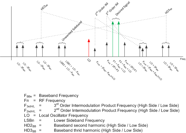
Graphical illustration of the modulator output spectrum with two tones is shown in Figure 1.
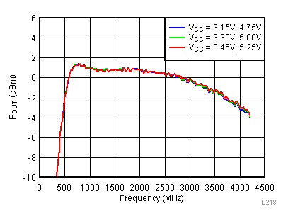
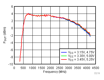
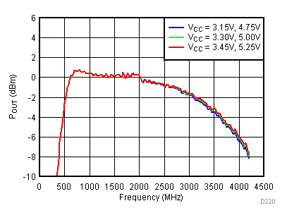
6.7 Typical Characteristics - Output Power
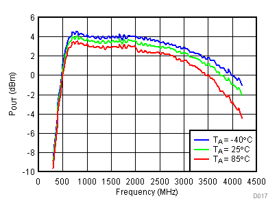
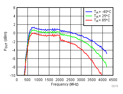
Unless specified all plots were created using TRF3722EVM, VCC = 3.3 V, VCC_TK = 5 V, TA = 25°C, I/Q frequency (fBB) 4.5 MHz and 5.5 MHz, 500 mVPP, VCM = 0.25 V, and 4.7 pF series capacitor at RFOUT. Optimized bias settings as per Table 16. Total Pout is two tones combined power.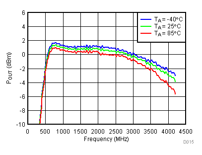
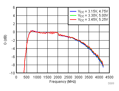
6.8 Typical Characteristics - Gain
Unless specified all plots were created using TRF3722EVM, VCC = 3.3 V, VCC_TK = 5 V, TA = 25°C, I/Q frequency (fBB) 4.5 MHz and 5.5 MHz, VCM = 0.25 V, and 4.7 pF series capacitor at RFOUT. Optimized bias settings as per Table 16.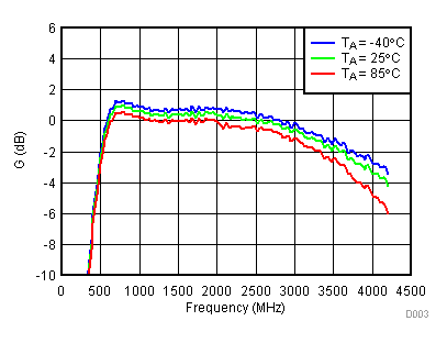
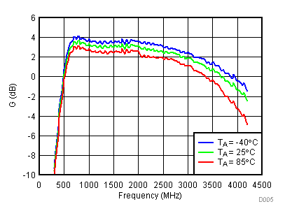
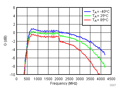
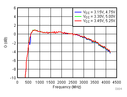
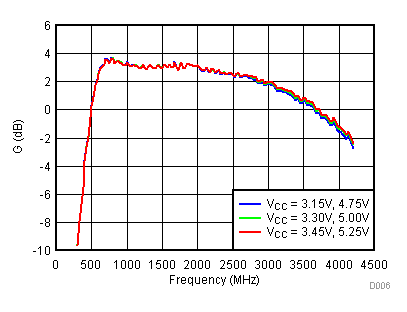
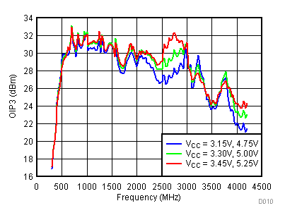
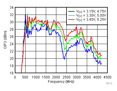
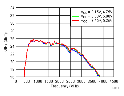
6.9 Typical Characteristics - OIP3
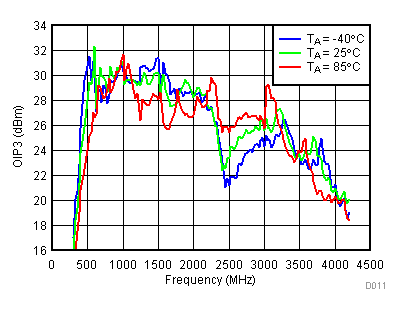
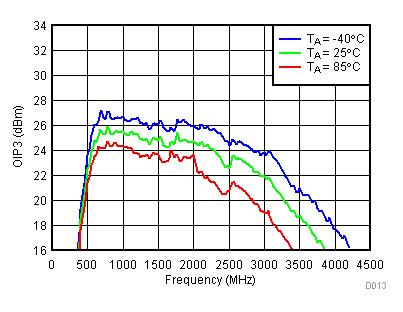
Unless specified all plots were created using TRF3722EVM, VCC = 3.3 V, VCC_TK = 5 V, TA = 25°C, I/Q frequency (fBB) 4.5 MHz and 5.5 MHz, VCM = 0.25 V, and 4.7 pF series capacitor at RFOUT. Optimized bias settings as per Table 16. Reported OIP3 is minimum of low side and high side.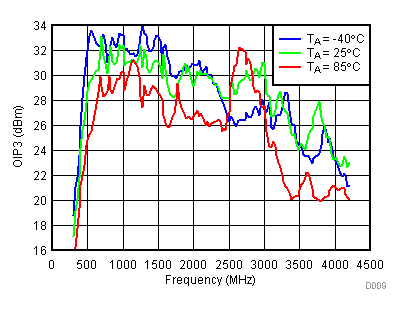
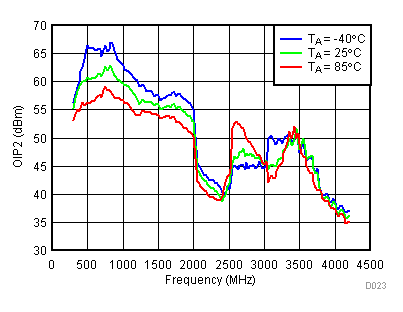
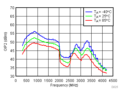
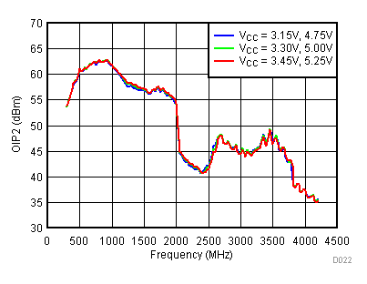
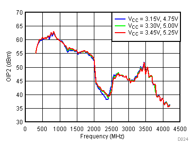
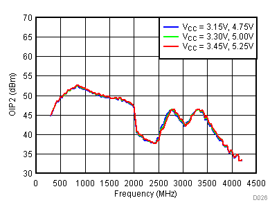
6.10 Typical Characteristics - OIP2
Unless specified all plots were created using TRF3722EVM, VCC = 3.3 V, VCC_TK = 5 V, TA = 25°C, I/Q frequency (fBB) 4.5 MHz and 5.5 MHz, VCM = 0.25 V, and 4.7 pF series capacitor at RFOUT. Optimized bias settings as per Table 16. Reported OIP2 is minimum of low side and high side.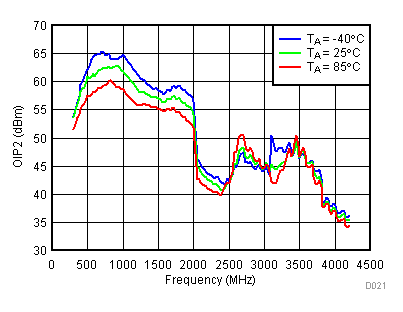
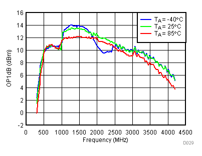
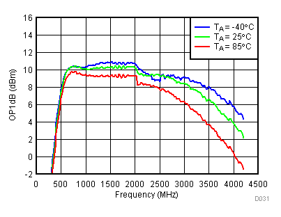
6.11 Typical Characteristics - OP1dB
Unless specified all plots were created using TRF3722EVM, VCC = 3.3 V, VCC_TK = 5 V, TA = 25°C, I/Q frequency (fBB) 5 MHz, VCM = 0.25 V, and 4.7 pF series capacitor at RFOUT. Optimized bias settings as per Table 16.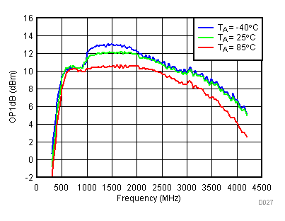
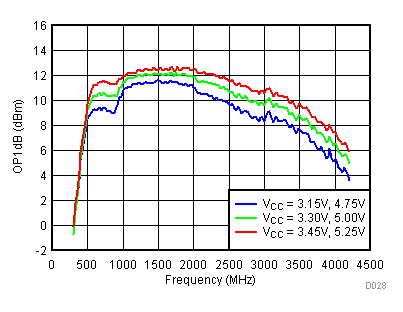
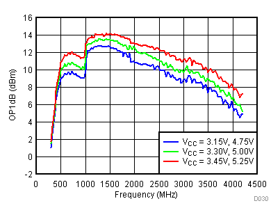
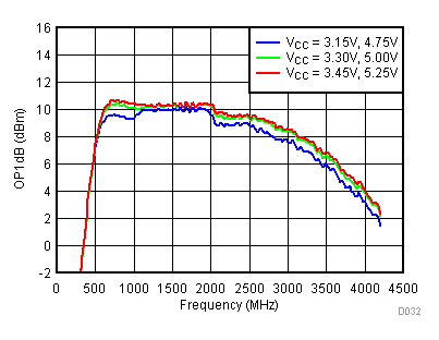
6.12 Typical Characteristics - Noise
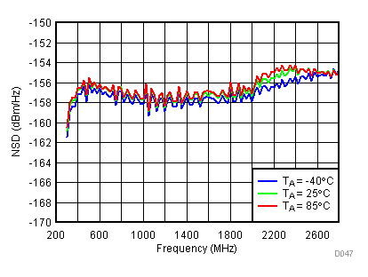
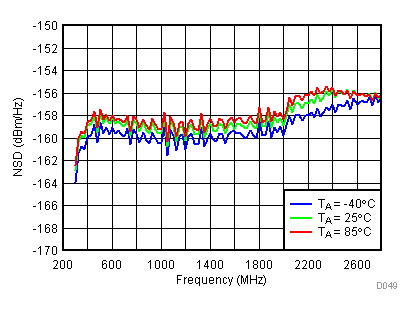
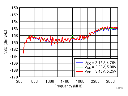
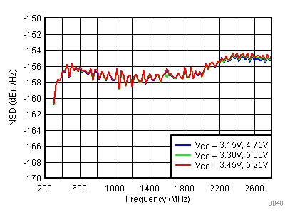
Unless specified all plots were created using TRF3722EVM, VCC = 3.3 V, VCC_TK = 5 V, TA = 25°C, BB inputs terminated to 50 Ω and 4.7 pF series capacitor at RFOUT. Optimized bias settings as per Table 16.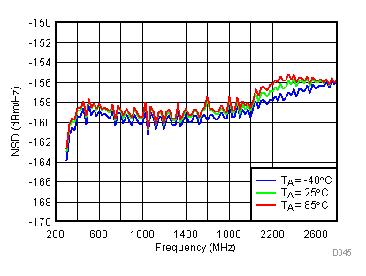
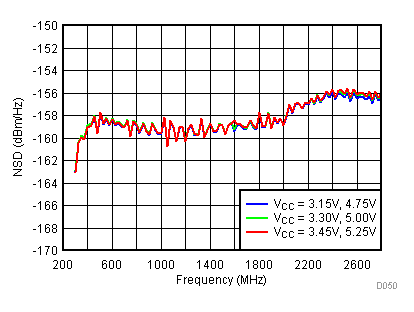
6.13 Typical Characteristics - Unadjusted CF
Unless specified all plots were created using TRF3722EVM, VCC = 3.3 V, VCC_TK= 5 V, TA = 25°C, I/Q frequency (fBB) 4.5 MHz and 5.5 MHz, VCM = 0.25 V, and 4.7 pF series capacitor at RFOUT. Optimized bias settings as per Table 16.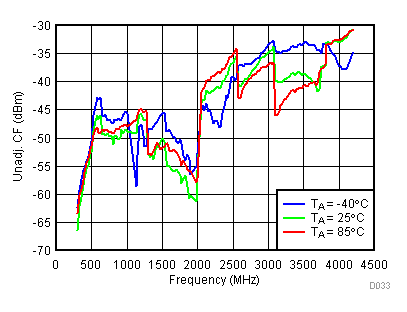 Figure 38. Unadjustable CF vs Temperature,
 Typical Operating Mode
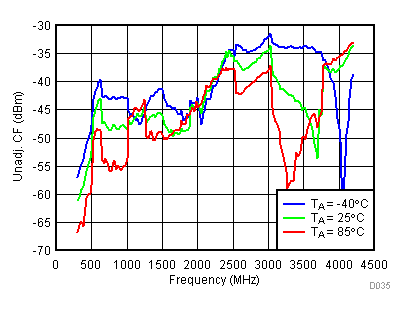
High Gain Mode
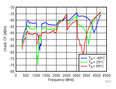
Low Power Mode
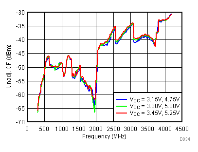 Figure 39. Unadjustable CF vs Supply,
 Typical Operating Mode
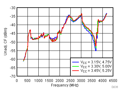
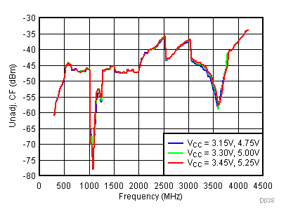
6.14 Typical Characteristics - Unadjusted SBS
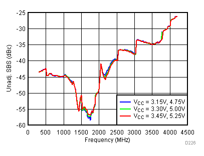
Unless specified all plots were created using TRF3722EVM, VCC = 3.3 V, VCC_TK= 5 V, and TA = 25°C, I/Q frequency (fBB) 4.5 MHz and 5.5 MHz, VCM = 0.25 V, and 4.7 pF series capacitor at RFOUT. Optimized bias settings as per Table 16.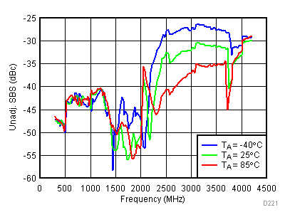 Figure 44. Unadjustable SBS vs Temperature,
 Typical Operating Mode
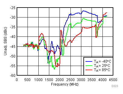
Temperature, High Gain Mode
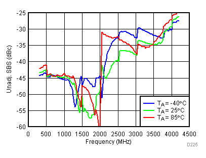
Low Power Mode
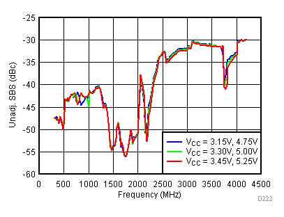 Figure 45. Unadjustable SBS vs Supply,
 Typical Operating Mode
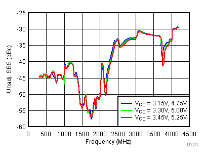
High Gain Mode
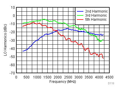
6.15 Typical Characteristics - LO Harmonic
Unless specified all plots were created using TRF3722EVM, VCC = 3.3 V, VCC_TK = 5 V, and TA = 25°C, I/Q frequency (fBB) 4.5 MHz and 5.5 MHz, VCM = 0.25 V, and 4.7 pF series capacitor at RFOUT. Optimized bias settings as per Table 16.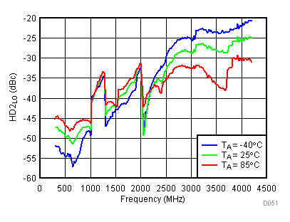 Figure 50. LO Second Harmonic vs Temperature,
 Typical Operating Mode
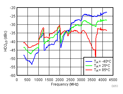 Figure 52. LO Second Harmonic vs Temperature,
 High Gain Mode
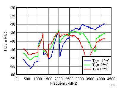 Figure 54. LO Second Harmonic vs Temperature,
 Low Power Mode
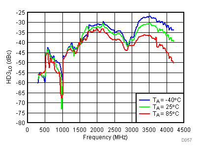 Figure 56. LO Third Harmonic vs Temperature,
 Typical Operating Mode
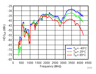 Figure 58. LO Third Harmonic vs Temperature,
 High Gain Mode
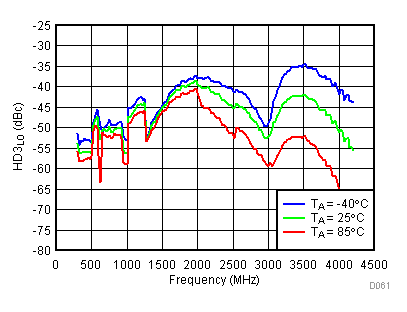 Figure 60. LO Third Harmonic vs Temperature,
 Low Power Mode
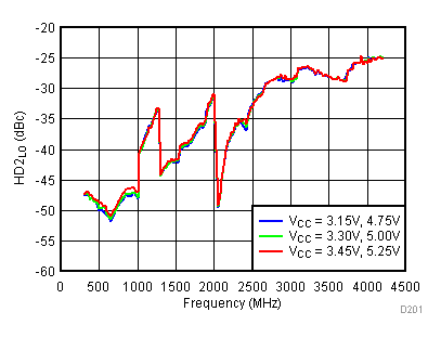 Figure 51. LO Second Harmonic vs Supply,
 Typical Operating Mode
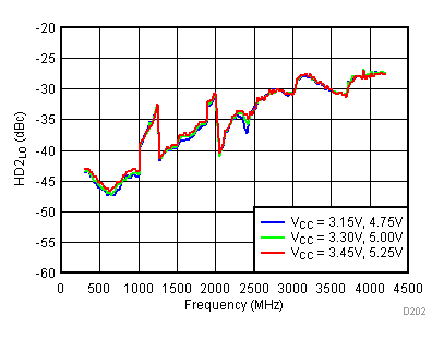 Figure 53. LO Second Harmonic vs Supply,
 High Gain Mode
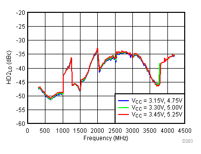 Figure 55. LO Second Harmonic vs Supply,
 Low Power Mode
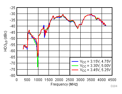 Figure 57. LO Third Harmonic vs Supply,
 Typical Operating Mode
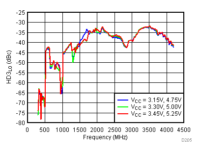 Figure 59. LO Third Harmonic vs Supply,
 High Gain Mode
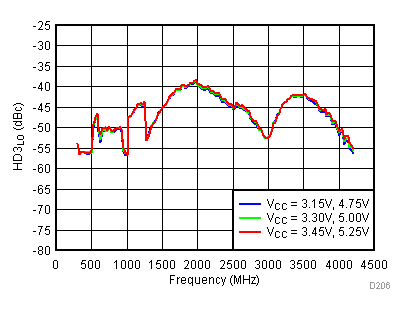 Figure 61. LO Third Harmonic vs Supply,
 Low Power Mode
6.16 Typical Characteristics - BB Harmonic
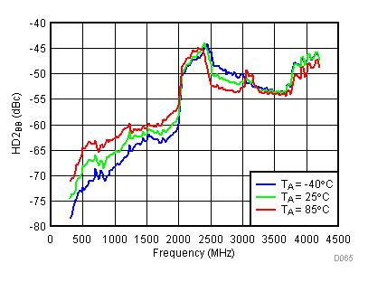
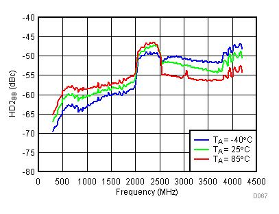
Unless specified all plots were created using TRF3722EVM, VCC = 3.3 V, VCC_TK= 5 V, and TA = 25°C, I/Q frequency (fBB) 4.5 MHz and 5.5 MHz, VCM = 0.25 V, and 4.7 pF series capacitor at RFOUT. Optimized bias settings as per Table 16. Reported BB harmonic is from (fBB) 4.5MHz.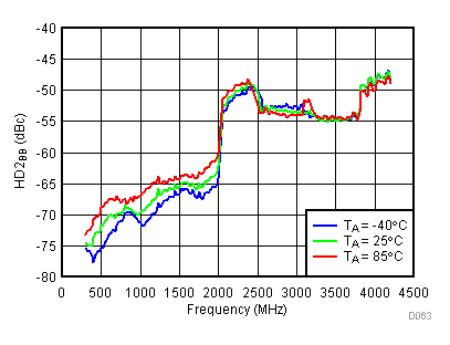
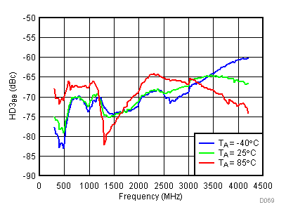
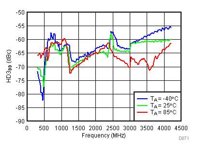
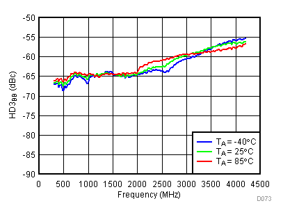
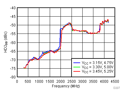
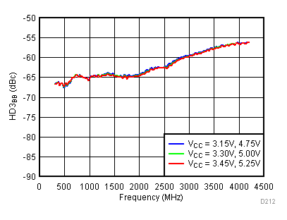
6.17 Typical Characteristics - RF Output Return Loss
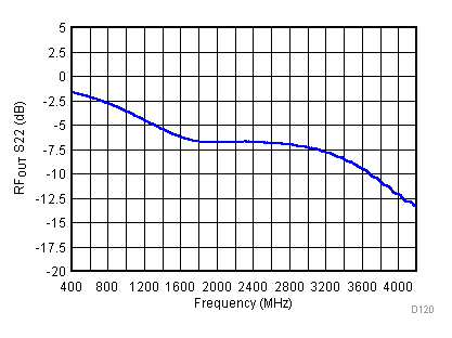
Unless specified all plots were created at RFOUT pin using TRF3722EVM, VCC = 3.3 V, VCC_TK = 5 V, and TA = 25°C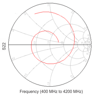 Figure 74. Smith Chart
6.18 Typical Characteristics - PLL/VCO
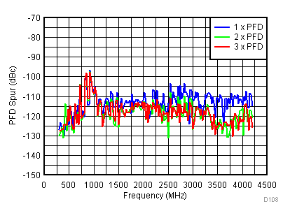
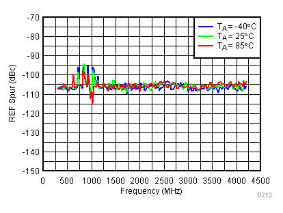
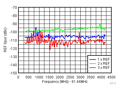
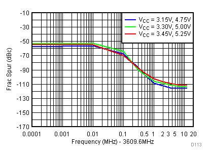
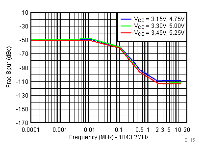
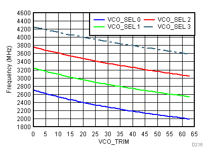
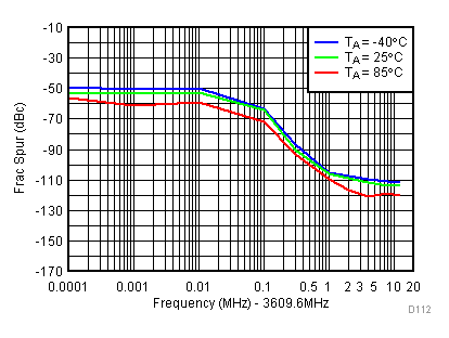
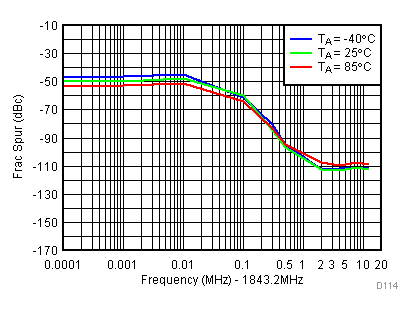
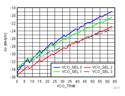
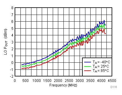
Unless specified all plots were created using TRF3722EVM, VCC = 3.3 V, VCC_TK = 5 V, and TA = 25°C. Measured at LO_OUTP with 50 Ω bias resistor and 47 pF series capacitor. Modulator section powered down. Reference frequency is set to 61.44 MHz. Optimized bias settings as per Table 16.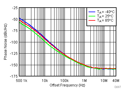 Figure 76. Open Loop Phase Noise at 450 MHz vs Temperature
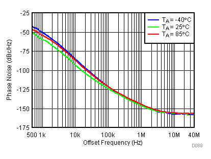
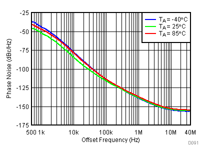
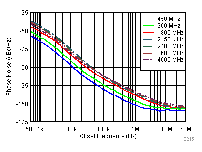
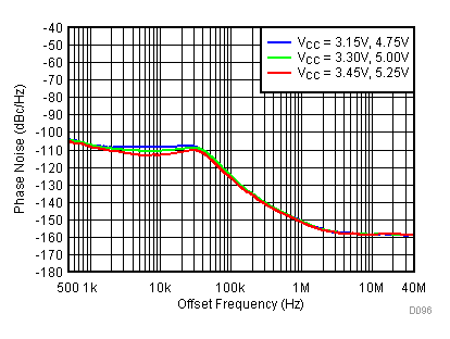 Figure 84. 450 MHz Frac-N (Closed Loop Phase Noise) vs Supply
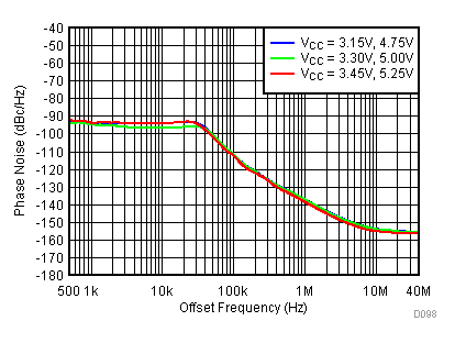 Figure 86. 1800 MHz Frac-N (Closed Loop Phase Noise) vs Supply
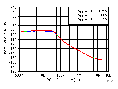 Figure 88. 2150 MHz Frac-N (Closed Loop Phase Noise) vs Supply
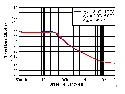 Figure 90. 2700 MHz Frac-N (Closed Loop Phase Noise) vs Supply
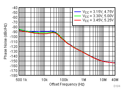 Figure 92. 3600 MHz Frac-N (Closed Loop Phase Noise) vs Supply
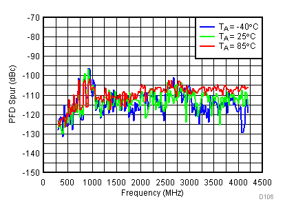 Figure 94. PFD Spur vs Temperature
| V(tune) = 1.1 V |
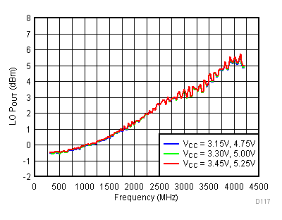
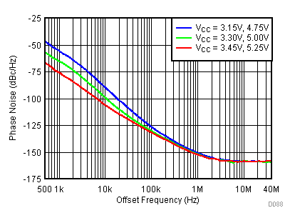 Figure 77. Open Loop Phase Noise at 450 MHz vs Supply
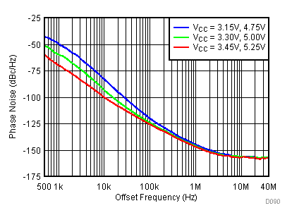
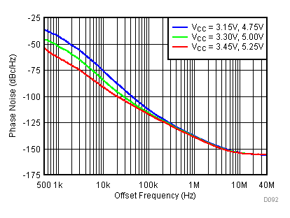
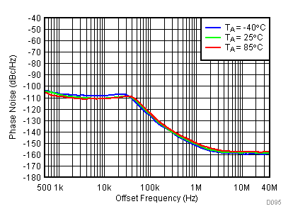
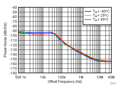 Figure 85. 1800 MHz Frac-N (Closed Loop Phase Noise) vs Temperature
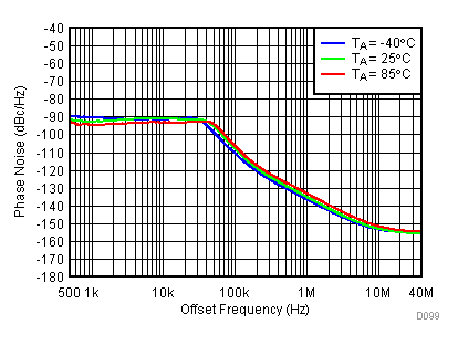 Figure 87. 2150 MHz Frac-N (Closed Loop Phase Noise) vs Temperature
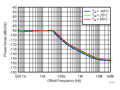 Figure 89. 2700 MHz Frac-N (Closed Loop Phase Noise) vs Temperature
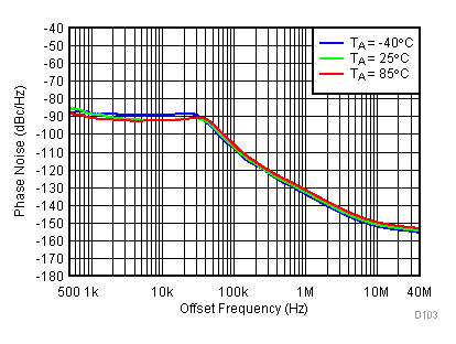 Figure 91. 3600 MHz Frac-N (Closed Loop Phase Noise) vs Temperature
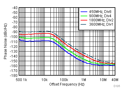 Figure 93. 450, 900, 1800, 3600 MHz Closed Loop Phase Noise vs Offset Frequency
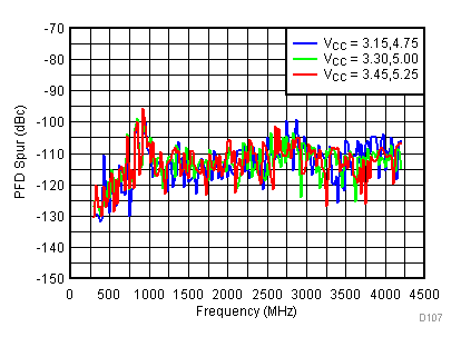 Figure 95. PFD Spur vs Supply
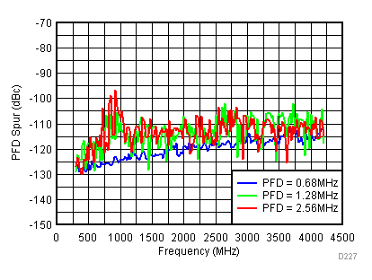
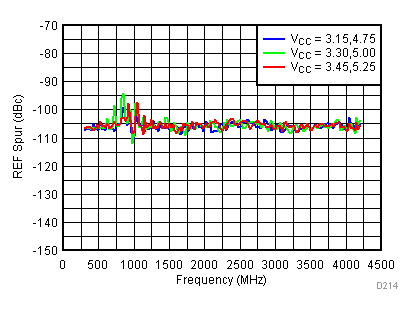
| V(tune) = 1.1 V |
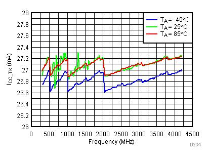
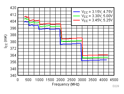
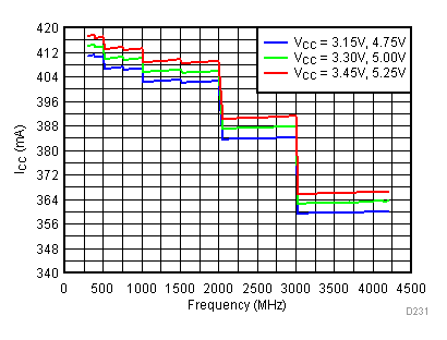
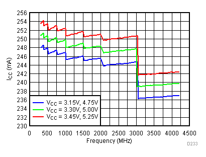
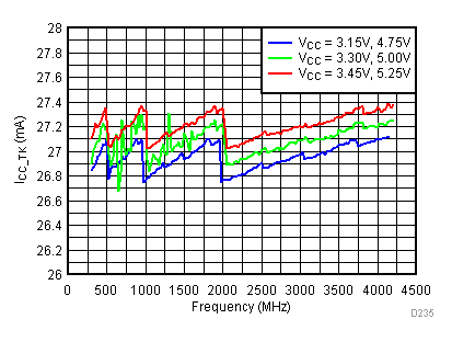
6.19 Typical Characteristics - Current Consumption
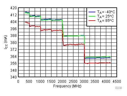
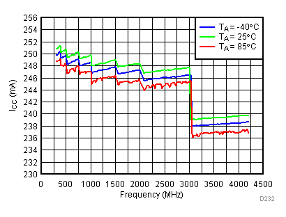
Unless specified all plots were created using TRF3722EVM, VCC = 3.3 V, VCC_TK = 5 V, and TA = 25°C. Optimized bias settings as per Table 16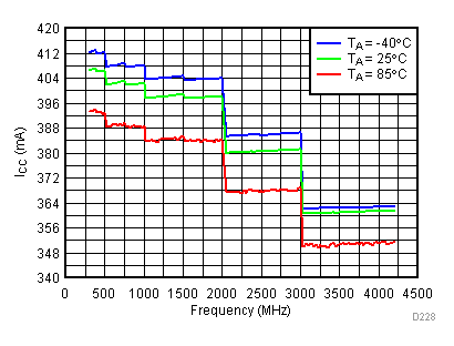
6.20 Typical Characteristics - Power Dissipation
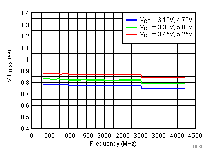
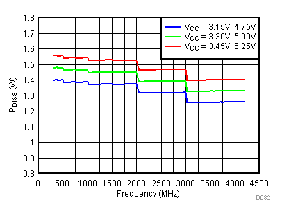
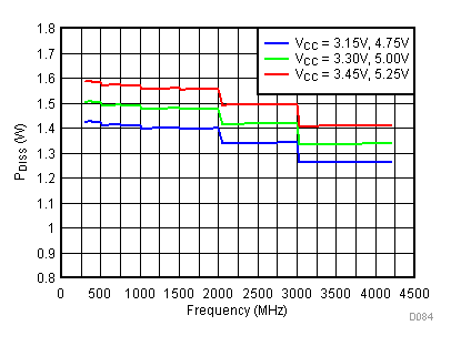
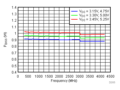
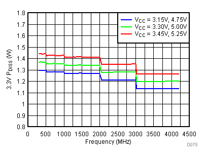
Unless specified all plots were created using TRF3722EVM, VCC = 3.3 V, VCC_TK = 5 V, and TA = 25°C. Optimized bias settings as per Table 16.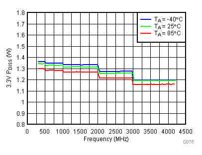 Figure 118. 3.3 V PDISS vs Temperature,
 Typical Operating Mode
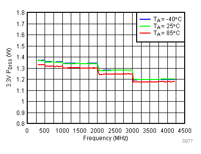
High Gain Mode
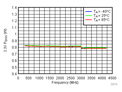
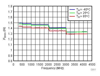
Typical Operating Mode
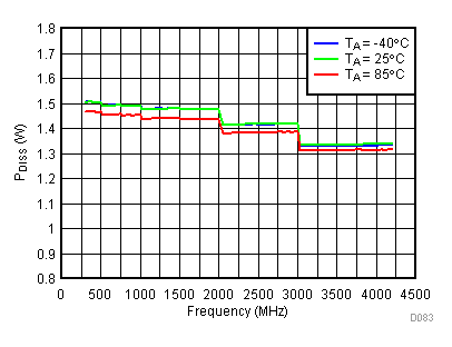
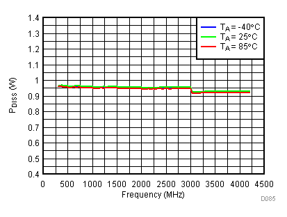
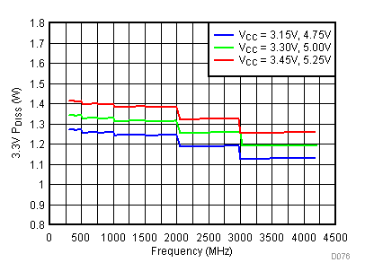 Figure 119. 3.3 V PDISS vs Supply,
 Typical Operating Mode
High Gain Mode
