SCDS371E January 2018 – April 2019 TS5MP646
PRODUCTION DATA.
- 1 Features
- 2 Applications
- 3 Description
- 4 Revision History
- 5 Pin Configuration and Functions
- 6 Specifications
- 7 Parameter Measurement Information
- 8 Detailed Description
- 9 Application and Implementation
- 10Power Supply Recommendations
- 11Layout
- 12Device and Documentation Support
- 13Mechanical, Packaging, and Orderable Information
Package Options
Mechanical Data (Package|Pins)
- YFP|36
Thermal pad, mechanical data (Package|Pins)
Orderable Information
8.3.2 1.8-V Logic Compatible Inputs
The TS5MP646 has 1.8-V logic compatible digital inputs for switch control. Regardless of the VDD voltage the digital input thresholds remained fixed, allowing a 1.8-V processor GPIO to control the TS5MP646 without the need for an external translator. This saves both space and BOM cost.
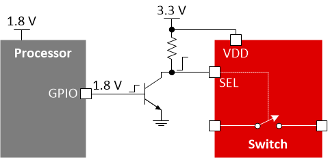
An example setup for a system without a 1.8-V logic compatible input is shown in Figure 22. Here the supply mismatch between the process and its GPIO output and the supply to the switch require a translator.
 Figure 22. System Without 1.8 V Logic Compatible Inputs
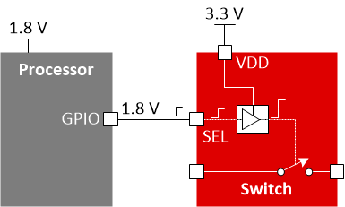
 With the 1.8 V logic compatibility in the TS5MP646, the translator is built in to the device so that the external components are no longer needed, simplifying the system design and overall cost.
 Figure 23. System With 1.8 V Logic Compatible Inputs