SCDS371E January   2018  – April 2019 TS5MP646

PRODUCTION DATA.  

  1. Features
  2. Applications
  3. Description
    1.     Device Images
      1.      Simplified D-PHY Schematic
      2.      Simplified C-PHY Schematic
  4. Revision History
  5. Pin Configuration and Functions
    1.     Pin Functions
  6. Specifications
    1. 6.1 Absolute Maximum Ratings
    2. 6.2 ESD Ratings
    3. 6.3 Recommended Operating Conditions
    4. 6.4 Thermal Information
    5. 6.5 Electrical Characteristics
    6. 6.6 Typical Characteristics
  7. Parameter Measurement Information
  8. Detailed Description
    1. 8.1 Overview
    2. 8.2 Functional Block Diagram
    3. 8.3 Feature Description
      1. 8.3.1 Powered-Off Protection
      2. 8.3.2 1.8-V Logic Compatible Inputs
      3. 8.3.3 Low Power Disable Mode
    4. 8.4 Device Functional Modes
      1. 8.4.1 Pin Functions
      2. 8.4.2 Low Power Disable Mode
      3. 8.4.3 Switch Enabled Mode
  9. Application and Implementation
    1. 9.1 Application Information
    2. 9.2 Typical Application
      1. 9.2.1 Design Requirements
      2. 9.2.2 Detailed Design Procedure
      3. 9.2.3 Application Curves
        1. 9.2.3.1 MIPI D-PHY Application
        2. 9.2.3.2 MIPI C-PHY Application
  10. 10Power Supply Recommendations
  11. 11Layout
    1. 11.1 Layout Guidelines
    2. 11.2 Layout Example
  12. 12Device and Documentation Support
    1. 12.1 Documentation Support
    2. 12.2 Receiving Notification of Documentation Updates
    3. 12.3 Community Resources
    4. 12.4 Trademarks
    5. 12.5 Electrostatic Discharge Caution
    6. 12.6 Glossary
  13. 13Mechanical, Packaging, and Orderable Information

Package Options

Mechanical Data (Package|Pins)
Thermal pad, mechanical data (Package|Pins)
Orderable Information

Typical Characteristics

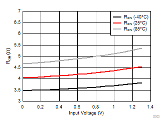
TS5MP646 D001_scds371.gif
Figure 1. RON vs Input Voltage. VDD = 1.65 V
TS5MP646 D003_scds371.gif
Figure 3. RON vs Input Voltage. VDD = 5.5 V
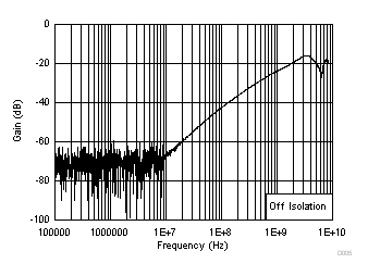
TS5MP646 D005_OSIO_scds371.gif
Figure 5. Off Isolation
TS5MP646 D002_scds371.gif
Figure 2. RON vs Input Voltage. VDD = 3.3 V
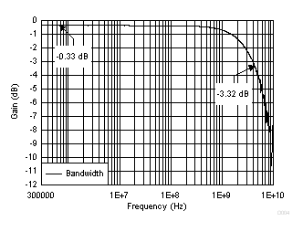
TS5MP646 D004_BW_scds371.gif
Figure 4. Differential Bandwidth
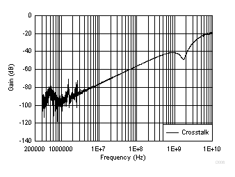
TS5MP646 D006_XTALK_scds371.gif
Figure 6. Differential Crosstalk