SLLSE67I March 2011 – March 2016 TUSB9261
PRODUCTION DATA.
- 1 Features
- 2 Applications
- 3 Description
- 4 Revision History
- 5 Pin Configuration and Functions
- 6 Specifications
- 7 Detailed Description
- 8 Application and Implementation
- 9 Power Supply Recommendations
- 10Layout
- 11Device and Documentation Support
- 12Mechanical, Packaging, and Orderable Information
Package Options
Mechanical Data (Package|Pins)
- PVP|64
Thermal pad, mechanical data (Package|Pins)
- PVP|64
Orderable Information
8 Application and Implementation
NOTE
Information in the following applications sections is not part of the TI component specification, and TI does not warrant its accuracy or completeness. TI’s customers are responsible for determining suitability of components for their purposes. Customers should validate and test their design implementation to confirm system functionality.
8.1 Application Information
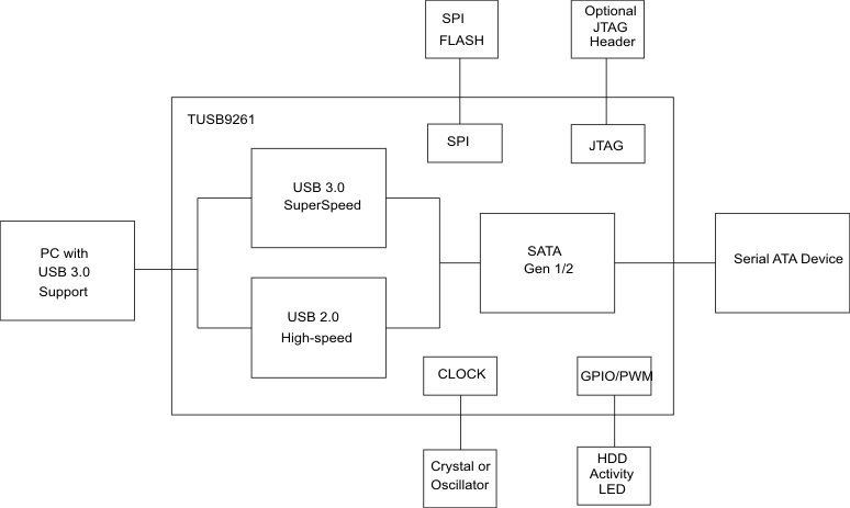
The device serves as a bridge between a downstream USB 3.0 host port and a SATA device such as a hard disk drive. A crystal or oscillator supplies the required clock source. A SPI flash device contains the firmware that is loaded into the TUSB9261 after the deassertion of RESET. Push buttons or any other desired logic can be connected to the TUSB9261 GPIO pins. The TUSB9261 can also output a pulse-width modulated signal that can be used to drive an activity LED.
8.2 Typical Application
 Figure 2. Typical Application Schematic
8.2.1 Design Requirements
Table 2. Design Parameters
| DESIGN PARAMETER | EXAMPLE VALUE |
|---|---|
| VDD supply | 1.1 V |
| VDD33 supply | 3.3 V |
| Upstream port USB support | SS, HS, FS |
| Main supply | VBUS |
| USB_VBUS resistor values | 90.9 kΩ, 10 kΩ |
| Crystal frequency | 40 MHz |
| SATA device | SSD |
8.2.2 Detailed Design Procedure
8.2.2.1 PWM Terminals
The TUSB9261 has two pulse-width modulated output terminals.
Table 3 shows the default firmware configuration of PWMs.
Table 3. Default Firmware Configuration of PWMs
PWM duty cycle will be 0% when the LED should be fully ON.
8.2.2.2 JTAG Interface
The TUSB9261 supports JTAG for board-level test and debug support. Typically, these terminals are left unconnected or routed to a header to plug in an external JTAG controller. Table 4 shows the JTAG terminal names and internal resistor connection. The JTAG interface should be left unconnected if JTAG support is not required.
Table 4. Internal JTAG Resistor Termination
| NAME | PULL UP OR PULL DOWN | DESCRIPTION |
|---|---|---|
| JTAG_TCK | Pull down | JTAG test clock |
| JTAG_TDI | Pull up | JTAG test data in |
| JTAG_TDO | Pull down | JTAG test data out |
| JTAG_TMS | Pull up | JTAG test mode select |
| JTAG_RSTZ | Pull down | JTAG reset |
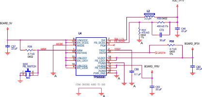
8.2.2.3 Voltage Regulator Schematic

8.2.2.4 SPI
A SPI system consists of one master device and one or more slave devices. The TUSB9261 is a SPI master providing the SPI clock, data-in, data-out, and up to three chip-select terminals.
The SPI has a 4-wire synchronous serial interface. Data communication is enabled with an active-low chip select terminal (SPI_CS[2:0]#). Data is transmitted with a 3-terminal interface consisting of terminals for serial data input (SPI_DATA_IN), serial data output (SPI_DATA_OUT) and serial clock (SPI_SCLK).
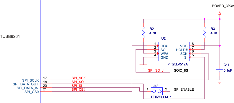
All SPI terminals have integrated pullup resistors. No external components are required to connect the SPI interface to an external SPI flash device. See Figure 3 for an example implementation of the SPI interface using one SPI slave device.
 Figure 3. SPI Connection
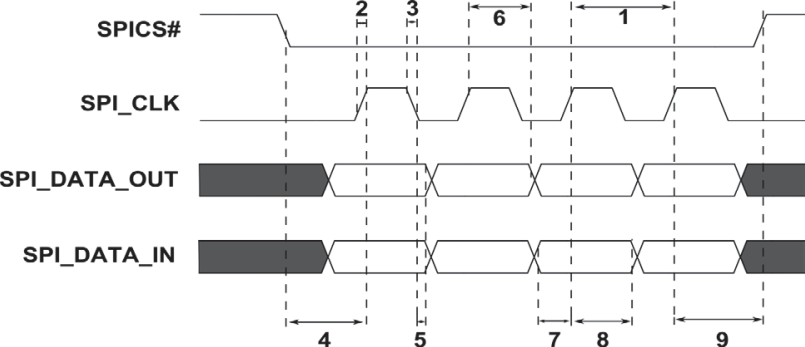
The SPI_CLK is running at a fixed frequency of 18.75 MHz and its clocking mode is configured with a POLARITY of 0 and a PHASE of 1, this means that the SPI sends the data output one half-cycle before the first rising edges of SPI_CLK and on subsequent falling edges. Meanwhile, the input data is latched on the rising edge of SPI_CLK (see Figure 4 and Table 5 for a detailed timing description).
The flash memory is erased by the bootloader prior to programming and must use a word size of 8 bits with an address length of 24 bits and its program instruction must allow 256 bytes to be written in one operation. TI recommends a minimum flash size of 512 kb (64 k × 8). Table 5 shows SPI flash devices that have been tested with the TUSB9261.
 Figure 4. SPI Characterization
Table 5. SPI Characterization Time
| NO. | TIME REFERENCE | THEORETICAL VALUE |
|---|---|---|
| 1 | Cycle time SPICLK | 53.3 ns |
| 2 | Positive SPI_CLK slope | 2 ns |
| 3 | Negative SPI_CLK slope | 3 ns |
| 4 | SPISCS – SPICLK edge(PHASE = 1) | MIN: 53.3 ns TYP: 80 ns MAX: 93.3 ns |
| 5 | Output delay time, SPICLK TX edge to SPISIMO valid | 260 ps |
| 6 | Output hold time, SPICLK RX edge to SPISIMO valid | 26.7 ns |
| 7 | Setup time | 22 ns |
| 8 | Hold time | 500 ps |
| 9 | "SPICLK -SPISCS Phase = 1, Master" | 13.3 ns |