SCES727B june 2008 – june 2023 TXB0104-Q1
PRODUCTION DATA
- 1
- 1 Features
- 2 Applications
- 3 Description
- 4 Revision History
- 5 Pin Configuration and Functions
-
6 Specifications
- 6.1 Absolute Maximum Ratings
- 6.2 ESD Ratings
- 6.3 Recommended Operating Conditions
- 6.4 Thermal Information
- 6.5 Electrical Characteristics
- 6.6 Timing Requirements: VCCA = 1.2 V
- 6.7 Timing Requirements: VCCA = 1.5 V ± 0.1 V
- 6.8 Timing Requirements: VCCA = 1.8 V ± 0.15 V
- 6.9 Timing Requirements: VCCA = 2.5 V ± 0.2 V
- 6.10 Timing Requirements: VCCA = 3.3 V ± 0.3 V
- 6.11 Switching Characteristics: VCCA = 1.2 V
- 6.12 Switching Characteristics: VCCA = 1.5 V ± 0.1 V
- 6.13 Switching Characteristics: VCCA = 1.8 V ± 0.15 V
- 6.14 Switching Characteristics: VCCA = 2.5 V ± 0.2 V
- 6.15 Switching Characteristics: VCCA = 3.3 V ± 0.3 V
- 6.16 Operating Characteristics
- 6.17 Typical Characteristics
- 7 Parameter Measurement Information
- 8 Detailed Description
- 9 Application and Implementation
- 10Power Supply Recommendations
- 11Layout
- 12Device and Documentation Support
- 13Mechanical, Packaging, and Orderable Information
Package Options
Mechanical Data (Package|Pins)
Thermal pad, mechanical data (Package|Pins)
Orderable Information
5 Pin Configuration and Functions
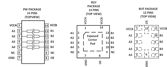
NC − No internal
connection
For RGY, if the
exposed center pad is used, it must be connected only to as a secondary ground
or left electrically open.
Table 5-1 Pin Functions
| PIN | I/O | DESCRIPTION | |
|---|---|---|---|
| NO. | NAME | ||
| 1 | VCCA | I | A-port supply voltage 1.2 V ≤ VCCA ≤ 3.6 V and VCCA ≤ VCCB. |
| 2 | A1 | I/O | Input/output 1. Referenced to VCCA. |
| 3 | A2 | I/O | Input/output 2. Referenced to VCCA. |
| 4 | A3 | I/O | Input/output 3. Referenced to VCCA. |
| 5 | A4 | I/O | Input/output 4. Referenced to VCCA. |
| 6 | NC | – | No connection. Not internally connected. |
| 7 | GND | – | Ground |
| 8 | OE | I | 3-state output-mode enable. Pull OE low to place all outputs in 3-state mode. Referenced to VCCA. |
| 9 | NC | – | No connection. Not internally connected. |
| 10 | B4 | I/O | Input/output 4. Referenced to VCCB. |
| 11 | B3 | I/O | Input/output 3. Referenced to VCCB. |
| 12 | B2 | I/O | Input/output 2. Referenced to VCCB. |
| 13 | B1 | I/O | Input/output 1. Referenced to VCCB. |
| 14 | VCCB | I | B-port supply voltage 1.65 V ≤ VCCB ≤ 5.5 V. |