SCES853E November 2013 – October 2023 TXS0104E-Q1
PRODUCTION DATA
- 1
- 1 Features
- 2 Applications
- 3 Description
- 4 Revision History
- 5 Pin Configuration and Functions
-
6 Specifications
- 6.1 Absolute Maximum Ratings
- 6.2 ESD Ratings
- 6.3 Recommended Operating Conditions
- 6.4 Thermal Information
- 6.5 Electrical Characteristics
- 6.6 Timing Requirements—VCCA = 1.8 V ± 0.15 V
- 6.7 Timing Requirements—VCCA = 2.5 V ± 0.2 V
- 6.8 Timing Requirements—VCCA = 3.3 V ± 0.3 V
- 6.9 Switching Characteristics—VCCA = 1.8 V ± 0.15 V
- 6.10 Switching Characteristics—VCCA = 2.5 V ± 0.2 V
- 6.11 Switching Characteristics—VCCA = 3.3 V ± 0.3 V
- 6.12 Typical Characteristics
- 7 Parameter Measurement Information
- 8 Detailed Description
- 9 Application and Implementation
- 10Device and Documentation Support
- 11Electrostatic Discharge Caution
- 12Glossary
- 13Mechanical, Packaging, and Orderable Information
Package Options
Refer to the PDF data sheet for device specific package drawings
Mechanical Data (Package|Pins)
- RUT|12
- PW|14
- BQA|14
Thermal pad, mechanical data (Package|Pins)
Orderable Information
8.3.1 Architecture
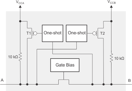
The TXS0104E-Q1 architecture (see Figure 8-1) does not require a direction-control signal in order to control the direction of data flow from A to B or from B to A.
 Figure 8-1 Architecture of a TXS01xx Cell
Each A-port I/O has an internal 10-kΩ pullup resistor to VCCA, and each B-port I/O has an internal 10-kΩ pullup resistor to VCCB. The output one-shots detect rising edges on the A or B ports. During a rising edge, the one-shot turns on the PMOS transistors (T1, T2) for a short duration which speeds up the low-to-high transition.