SCES861E June 2015 – April 2024 TXS0108E-Q1
PRODUCTION DATA
- 1
- 1 Features
- 2 Applications
- 3 Description
- 4 Pin Configuration and Functions
-
5 Specifications
- 5.1 Absolute Maximum Ratings
- 5.2 ESD Ratings
- 5.3 Recommended Operating Conditions
- 5.4 Thermal Information
- 5.5 Electrical Characteristics: TA = –40°C to 125°C
- 5.6 Timing Requirements: VCCA = 1.5V ± 0.1 V
- 5.7 Timing Requirements: VCCA = 1.8V ± 0.15V
- 5.8 Timing Requirements: VCCA = 2.5V ± 0.2V
- 5.9 Timing Requirements: VCCA = 3.3V ± 0.3V
- 5.10 Switching Characteristics: VCCA = 1.5V ± 0.1V
- 5.11 Switching Characteristics: VCCA = 1.8V ± 0.15V
- 5.12 Switching Characteristics: VCCA = 2.5V ± 0.2V
- 5.13 Switching Characteristics: VCCA = 3.3V ± 0.3V
- 5.14 Typical Characteristics
- 6 Parameter Measurement Information
- 7 Detailed Description
- 8 Application and Implementation
- 9 Device and Documentation Support
- 10Revision History
- 11Mechanical, Packaging, and Orderable Information
Package Options
Refer to the PDF data sheet for device specific package drawings
Mechanical Data (Package|Pins)
- RKS|20
- PW|20
Thermal pad, mechanical data (Package|Pins)
- PW|20
Orderable Information
7.3.1 Architecture
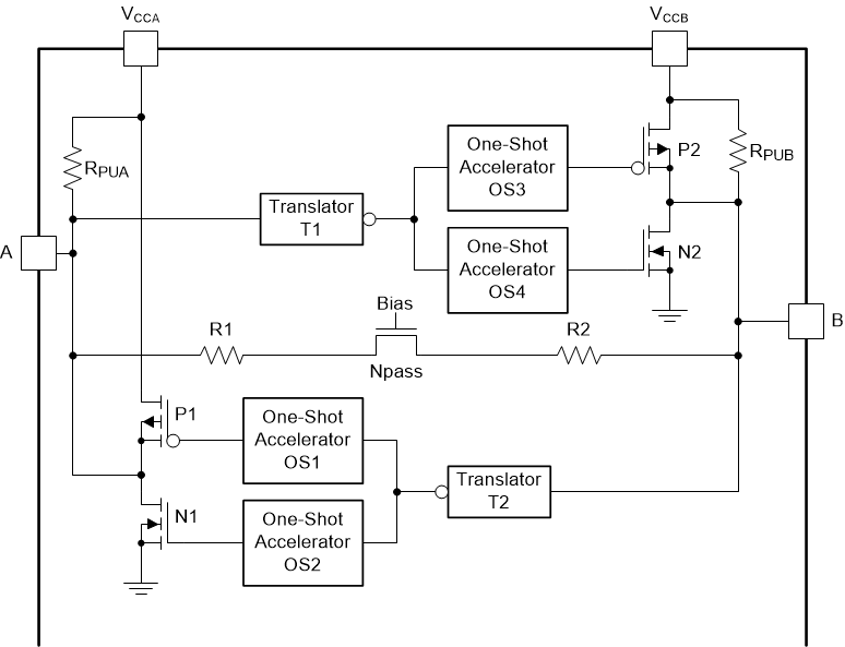
Figure 7-1 shows semi-buffered architecture design this application requires for both push-pull and open-drain mode. This application uses edge-rate accelerator circuitry (for both the high-to-low and low-to-high edges), a high-on-resistance N-channel pass-gate transistor (on the order of 300Ω to 500Ω) and pull-up resistors (to provide DC-bias and drive capabilities) to meet these requirements. This design does not need a direction-control signal to control the direction of data flow from A to B or from B to A. The resulting implementation supports both low-speed open-drain operation as well as high-speed push-pull operation.
 Figure 7-1 Architecture of a TXS0108E-Q1 Cell
When transmitting data from A-ports to B-ports, during a rising edge the one-shot circuit (OS3) turns on the PMOS transistor (P2) for a short-duration which reduces the low-to-high transition time. Similarly, during a falling edge, when transmitting data from A to B, the one-shot circuit (OS4) turns on the N-channel MOSFET transistor (N2) for a short-duration which speeds up the high-to-low transition. The B-port edge-rate accelerator consists of one-shot circuits OS3 and OS4. Transistors P2 and N2 and serves to rapidly force the B port high or low when a corresponding transition is detected on the A port.
When transmitting data from B- to A-ports, during a rising edge the one-shot circuit (OS1) turns on the PMOS transistor (P1) for a short-duration which reduces the low-to-high transition time. Similarly, during a falling edge, when transmitting data from B to A, the one-shot circuit (OS2) turns on NMOS transistor (N1) for a short-duration and this speeds up the high-to-low transition. The A-port edge-rate accelerator consists of one-shots OS1 and OS2, transistors P1 and N1 components and form the edge-rate accelerator and serves to rapidly force the A port high or low when a corresponding transition is detected on the B port.