SLUSDD5A April   2019  – December 2020 UC1825B-SP

PRODUCTION DATA  

  1. Features
  2. Applications
  3. Description
  4. Revision History
  5. Pin Configuration and Functions
  6. Specifications
    1. 6.1 Absolute Maximum Ratings
    2. 6.2 ESD Ratings
    3. 6.3 Recommended Operating Conditions
    4. 6.4 Thermal Information
    5. 6.5 Electrical Characteristics
    6. 6.6 Typical Characteristics
  7. Detailed Description
    1. 7.1 Overview
    2. 7.2 Functional Block Diagram
    3. 7.3 Feature Description
      1. 7.3.1 Control Methods
      2. 7.3.2 Synchronization
      3. 7.3.3 High Current Outputs
      4. 7.3.4 Open Loop Test Circuit
    4. 7.4 Device Functional Modes
  8. Application and Implementation
    1. 8.1 Application Information
    2. 8.2 Typical Application
      1. 8.2.1 System Design Theory
        1. 8.2.1.1 Switching Frequency
        2. 8.2.1.2 Transformer
        3. 8.2.1.3 RCD and Diode Clamp
        4. 8.2.1.4 Output Diode
        5. 8.2.1.5 Main Switching MOSFETs
        6. 8.2.1.6 Output Filter and Capacitance
        7. 8.2.1.7 Compensation
        8. 8.2.1.8 Sense Resistor
    3. 8.3 Application Curves
  9. Power Supply Recommendations
  10. 10Layout
    1. 10.1 Layout Guidelines
      1. 10.1.1 Feedback Traces
      2. 10.1.2 Input/Output Capacitors
      3. 10.1.3 Compensation Components
      4. 10.1.4 Traces and Ground Planes
      5. 10.1.5 Ground Planes
    2. 10.2 Layout Example
  11. 11Device and Documentation Support
    1. 11.1 Documentation Support
      1. 11.1.1 Related Documentation
    2. 11.2 Receiving Notification of Documentation Updates
    3. 11.3 Support Resources
    4. 11.4 Trademarks
    5. 11.5 Electrostatic Discharge Caution
    6. 11.6 Glossary
  12. 12Mechanical, Packaging, and Orderable Information

Package Options

Mechanical Data (Package|Pins)
Thermal pad, mechanical data (Package|Pins)
Orderable Information

Synchronization

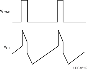
The oscillator can be synchronized by an external pulse inserted in series with the timing capacitor (see Figure 7-2). Program the free running frequency of the oscillator to be 10% to 15% slower than the desired synchronous frequency. The pulse width must be greater than 10 ns and less than half the discharge time of the oscillator. Figure 7-3 shows how to synchronize two ICs, with one as primary and one as secondary. Figure 7-4 shows the waveforms in a primary and secondary configuration.
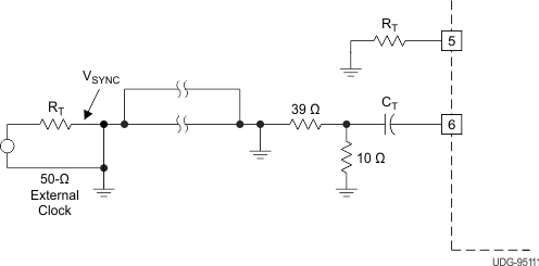
GUID-55879AA1-AB3E-4A89-B707-49BE147E748F-low.gifFigure 7-2 General Oscillator Synchronization
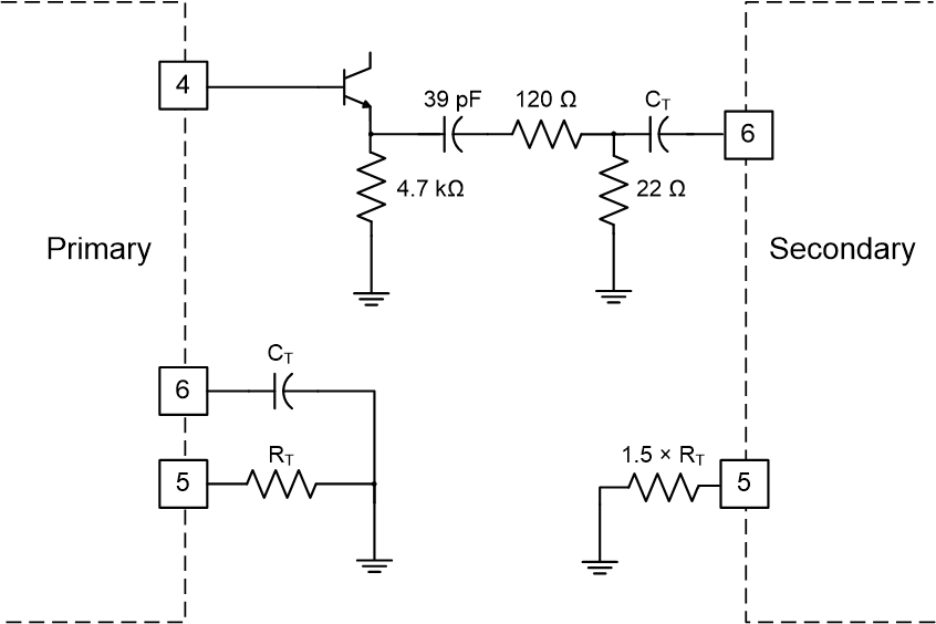
GUID-20201015-CA0I-KVT6-R30X-QGKWN3XGSXGZ-low.gif Figure 7-3 Two Unit Interface
GUID-E55865B3-2313-4F8D-8E0F-EBF262C2DD17-low.gifFigure 7-4 Operational Waveforms