SLUSDD5A April 2019 – December 2020 UC1825B-SP
PRODUCTION DATA
- 1 Features
- 2 Applications
- 3 Description
- 4 Revision History
- 5 Pin Configuration and Functions
- 6 Specifications
- 7 Detailed Description
- 8 Application and Implementation
- 9 Power Supply Recommendations
- 10Layout
- 11Device and Documentation Support
- 12Mechanical, Packaging, and Orderable Information
Package Options
Mechanical Data (Package|Pins)
- HKT|16
- KGD|0
Thermal pad, mechanical data (Package|Pins)
Orderable Information
8.2 Typical Application
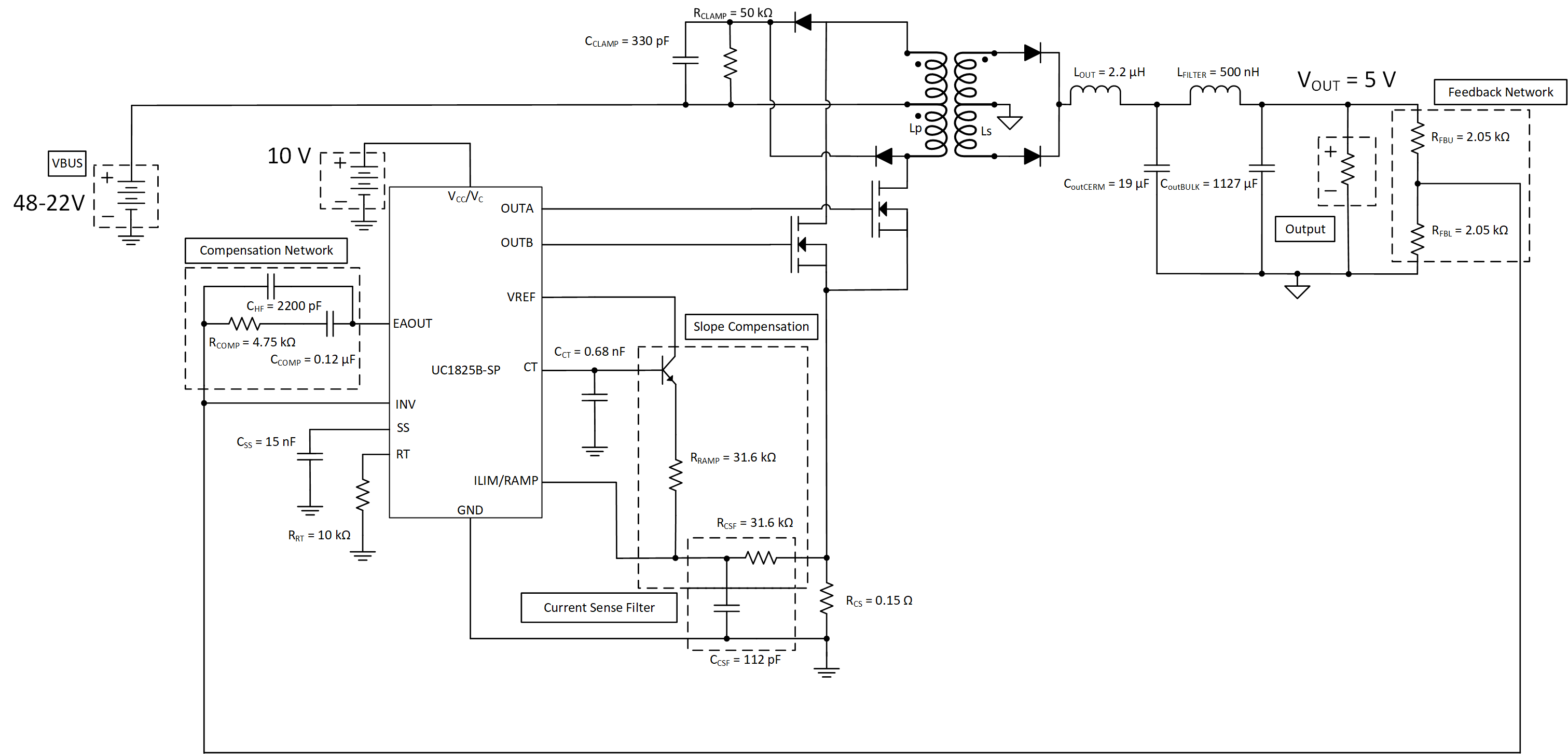
The UC1825B-SP as a dual output controller that has integrated drivers for a push-pull topology and can be used for half bridge and full bridge applications by using external high side drivers. While the UC1825B-SP originally supported voltage mode topologies, the device with minimal external components can support current mode topologies as well. The RAMP pin is used for the input current sense and the ILIM pin is used as the current limit pin. External components are needed to ensure slope compensation is implemented.
 Figure 8-4 Typical Application
Table 8-1 Design Parameters
| PARAMETER | SPECIFICATIONS |
|---|---|
| Input Power Supply | 22 to 48 VDC |
| Output Voltage | 5 VDC |
| Output Current | 0 to 10 A |
| Output Current Pre-load | 0.5 mA |
| Operating Temperature | 25°C |
| Switching Frequency of UC1825B-SP | 215 kHz |
| Peak Input Current Limit | 7 A |
| Bandwidth | ~5 kHz |
| Phase Margin | ~80° |