SLUSD49A September 2017 – January 2019 UCC256303
PRODUCTION DATA.
- 1 Features
- 2 Applications
- 3 Description
- 4 Revision History
- 5 Pin Configuration and Functions
- 6 Specifications
-
7 Detailed Description
- 7.1 Overview
- 7.2 Functional Block Diagram
- 7.3
Feature Description
- 7.3.1 Hybrid Hysteretic Control
- 7.3.2 Regulated 12-V Supply
- 7.3.3 Feedback Chain
- 7.3.4 Optocoupler Feedback Signal Input and Bias
- 7.3.5 System External Shut Down
- 7.3.6 Pick Lower Block and Soft Start Multiplexer
- 7.3.7 Pick Higher Block and Burst Mode Multiplexer
- 7.3.8 VCR Comparators
- 7.3.9 Resonant Capacitor Voltage Sensing
- 7.3.10 Resonant Current Sensing
- 7.3.11 Bulk Voltage Sensing
- 7.3.12 Output Voltage Sensing
- 7.3.13 High Voltage Gate Driver
- 7.3.14 Protections
- 7.4 Device Functional Modes
-
8 Application and Implementation
- 8.1 Application Information
- 8.2
Typical Application
- 8.2.1 Design Requirements
- 8.2.2
Detailed Design Procedure
- 8.2.2.1 LLC Power Stage Requirements
- 8.2.2.2 LLC Gain Range
- 8.2.2.3 Select Ln and Qe
- 8.2.2.4 Determine Equivalent Load Resistance
- 8.2.2.5 Determine Component Parameters for LLC Resonant Circuit
- 8.2.2.6 LLC Primary-Side Currents
- 8.2.2.7 LLC Secondary-Side Currents
- 8.2.2.8 LLC Transformer
- 8.2.2.9 LLC Resonant Inductor
- 8.2.2.10 LLC Resonant Capacitor
- 8.2.2.11 LLC Primary-Side MOSFETs
- 8.2.2.12 Design Considerations for Adaptive Dead-Time
- 8.2.2.13 LLC Rectifier Diodes
- 8.2.2.14 LLC Output Capacitors
- 8.2.2.15 BLK Pin Voltage Divider
- 8.2.2.16 BW Pin Voltage Divider
- 8.2.2.17 ISNS Pin Differentiator
- 8.2.2.18 VCR Pin Capacitor Divider
- 8.2.2.19 Burst Mode Programming
- 8.2.2.20 Soft-Start Capacitor
- 8.2.3 Application Curves
- 9 Power Supply Recommendations
- 10Layout
- 11Device and Documentation Support
- 12Mechanical, Packaging, and Orderable Information
Package Options
Refer to the PDF data sheet for device specific package drawings
Mechanical Data (Package|Pins)
- DDB|14
Thermal pad, mechanical data (Package|Pins)
Orderable Information
9.2 Boot Capacitor
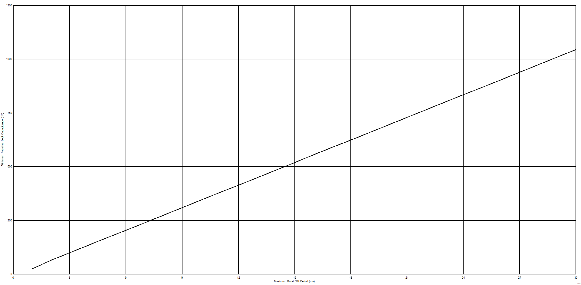
During burst off period, power consumed by the high side gate driver from the HB pin must be drawn from CBOOT and will cause its voltage to decay. At the start of the next burst period there must be sufficient voltage remaining on CBOOT to power the high side gate driver until the conduction period of LO allows it to be replenished from CRVCC. The power consumed by the high side driver during this burst off period will therefore have a direct impact on the size and cost of capacitors that must be connected to CBOOT and RVCC.
Assume the system has a maximum burst off period of 10 ms.

Assume the bootstrap diode has a forward voltage drop of 1 V:

Assume the boot voltage to be always above 8 V to avoid UVLO fault. Then the maximum allowed voltage drop on boot capacitor is:

Boot capacitor can then be sized:

 Figure 50. Minimum Required Boot Capacitance vs. Maximum Burst Off Period