SLUS704C FEBRUARY 2007 – December 2014 UCC27423-EP , UCC27424-EP
PRODUCTION DATA.
- 1 Features
- 2 Applications
- 3 Description
- 4 Revision History
- 5 Pin Configuration and Functions
- 6 Specifications
- 7 Detailed Description
- 8 Application and Implementation
- 9 Power Supply Recommendations
- 10Layout
- 11Device and Documentation Support
- 12Mechanical, Packaging, and Orderable Information
Package Options
Mechanical Data (Package|Pins)
- D|8
Thermal pad, mechanical data (Package|Pins)
Orderable Information
8 Application and Implementation
NOTE
Information in the following applications sections is not part of the TI component specification, and TI does not warrant its accuracy or completeness. TI’s customers are responsible for determining suitability of components for their purposes. Customers should validate and test their design implementation to confirm system functionality.
8.1 Application Information
UCC2742x-EP is designed for high-speed and high-operating reliability. UCC2742x family of gate driver is capable of delivering 4 A into capacitive load. Inverting outputs of UCC27423 are intended to drive external P-Channel MOSFETs and noninverting outputs of UCC27424 are intended to drive external N-channel MOSFETs.
8.2 Typical Application
Figure 24 shows typical application of UCC2742x device when used as a gate driver for the power MOSFET in boost converter application.
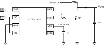 Figure 24. Typical Application Schematic
8.2.1 Design Requirements
When selecting the proper gate driver device for an end application, some design considerations must be evaluated first in order to make the most appropriate selection. Among these considerations are input-to-output configuration, input threshold type, bias supply voltage, peak source and sink current, availability of independent enable and disable function, propagation delay, power dissipation and package type.
Table 2. Design Parameters
| Parameters | Value |
|---|---|
| Supply voltage | 4.5 to 15 V |
| Output source current | 4 A |
| Output sink current | 4 A |
| Propagation delay | 25 ns |
| Rise time | 20 ns |
| Fall time | 15 ns |
8.2.2 Detailed Design Procedure
Propagation Delay:
The acceptable propagation delay from the gate driver is dependent on the switching frequency at which it is used and the acceptable level of pulse distortion to the system. The UCC2742x-EP device features 25 ns (typical) propagation delay which ensures very little pulse distortion and allows operation at high frequencies.
8.2.2.1 Source/Sink Capabilities During Miller Plateau
Large power MOSFETs present a large load to the control circuitry. Proper drive is required for efficient, reliable operation. The UCC2742x drivers are optimized to provide maximum drive to a power MOSFET during the Miller plateau region of the switching transition. This interval occurs while the drain voltage is swinging between the voltage levels dictated by the power topology, requiring the charging/discharging of the drain-gate capacitance with current supplied or removed by the driver device. [1]
Two circuits are used to test the current capabilities of the UCC27423 driver. In each case, external circuitry is added to clamp the output near 5 V while the IC is sinking or sourcing current. An input pulse of 250 ns is applied at a frequency of 1 kHz in the proper polarity for the respective test. Each test showed a transient period where the current peaked up and then settled down to a steady-state value. The noted current measurements are made 200 ns after the input pulse is applied, following the initial transient.
The first circuit in Figure 25 is used to verify the current sink capability when the output of the driver is clamped around 5 V (a typical value of gate-source voltage during the Miller plateau region). The UCC27423 is found to sink 4.5 A at VDD = 15 V and 4.28 A at VDD = 12 V.
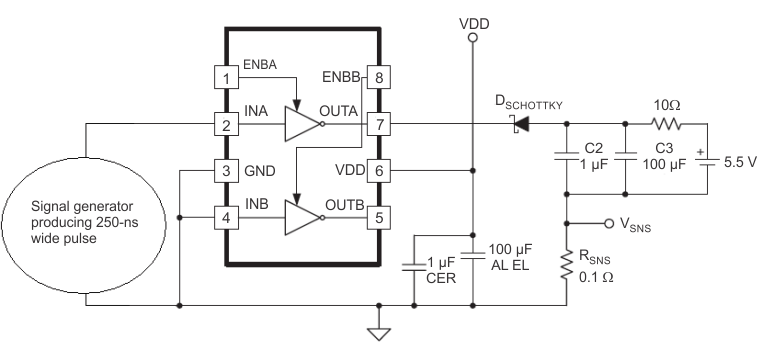
The circuit shown in Figure 26 is used to test the current source capability, with the output clamped to around
5 V with a string of Zener diodes. The UCC27423 is found to source 4.8 A at VDD = 15 V and 3.7 A at VDD =
12 V.
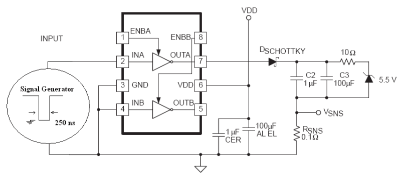
Note that the current sink capability is slightly stronger than the current source capability at lower VDD. This is due to the differences in the structure of the bipolar-MOSFET power output section, where the current source is a P-channel MOSFET, and the current sink has an N-channel MOSFET.
In most applications, it is advantageous that the turn-off capability of a driver is stronger than the turn-on capability. This helps ensure that the MOSFET is held OFF during common power-supply transients, which may turn the device back ON.
8.2.2.2 Parallel Outputs
The A and B drivers may be combined into a single driver by connecting the INA/INB inputs together and the OUTA/OUTB outputs together. Then, a single signal can control the paralleled combination as shown in Figure 27.
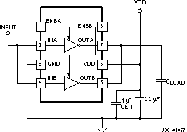 Figure 27. Parallel Outputs
8.2.3 Application Curve
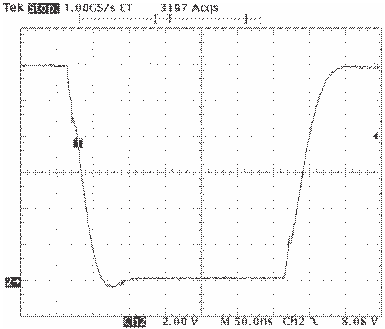 Figure 28. Pulse Response