SLUS704C FEBRUARY 2007 – December 2014 UCC27423-EP , UCC27424-EP
PRODUCTION DATA.
- 1 Features
- 2 Applications
- 3 Description
- 4 Revision History
- 5 Pin Configuration and Functions
- 6 Specifications
- 7 Detailed Description
- 8 Application and Implementation
- 9 Power Supply Recommendations
- 10Layout
- 11Device and Documentation Support
- 12Mechanical, Packaging, and Orderable Information
Package Options
Mechanical Data (Package|Pins)
- D|8
Thermal pad, mechanical data (Package|Pins)
Orderable Information
7 Detailed Description
7.1 Overview
High-frequency power supplies often require high-speed, high-current drivers such as the UCC2742x. A leading application of the UCC2742x provides a high-power buffer stage between the pulse-duration modulation (PWM) output of the control IC and the gates of the primary power MOSFET or insulated gate bipolar transistor (IGBT) switching devices. In other cases, the driver IC is used to drive the power-device gates through a drive transformer. Synchronous rectification supplies also have the need to simultaneously drive multiple devices, which can present an extremely-large load to the control circuitry.
Driver ICs are used when it is not feasible to have the primary PWM regulator IC directly drive the switching devices, for one or more reasons. The PWM IC may not have the brute drive capability required for the intended switching MOSFET, limiting the switching performance in the application. In other cases, there may be a desire to minimize the effect of high-frequency switching noise by placing the high-current driver physically close to the load. Also, newer ICs that target the highest operating frequencies may not incorporate onboard gate drivers at all. Their PWM outputs are intended to drive only the high-impedance input to drivers such as the UCC2742x. Finally, the control IC may be under thermal stress due to power dissipation, and an external driver can help by moving the heat from the controller to an external package.
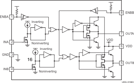
7.2 Functional Block Diagram
7.3 Feature Description
7.3.1 Input Stage
The input thresholds have a 3.3-V logic sensitivity over the full range of VDD voltages. However, they are equally compatible with 0 to VDD signals. The inputs of the UCC2742x are designed to withstand 500-mA reverse current without either damage to the IC or logic upset. The input stage of each driver should be driven by a signal with a short rise or fall time. This condition is satisfied in typical power-supply applications, where the input signals are provided by a PWM controller or logic gates with fast transition times (<200 ns). The input stages to the drivers function as a digital gate, and they are not intended for applications where a slow-changing input voltage is used to generate a switching output when the logic threshold of the input section is reached. While this may not be harmful to the driver, the output of the driver may switch repeatedly at a high frequency.
Users should not attempt to shape the input signals to the driver in an effort to slow down (or delay) the signal at the output. If limiting the rise or fall times to the power device is desired, limit the rise or fall times to the power device. Then, the user can add an external resistance between the output of the driver and the load device, which is generally a power MOSFET gate. The external resistor also may help remove power dissipation from the device package, as discussed in Thermal Considerations.
7.3.2 Output Stage
Inverting outputs of the UCC27423 are intended to drive external P-channel MOSFETs. Noninverting outputs of the UCC27424 are intended to drive external N-channel MOSFETs.
Each output stage is capable of supplying ±4-A peak current pulses and swings to both VDD and GND. The pullup/ pulldown circuits of the driver are constructed of bipolar and MOSFET transistors in parallel. The peak output current rating is the combined current from the bipolar and MOSFET transistors. The output resistance is the RDS(on) of the MOSFET transistor when the voltage on the driver output is less than the saturation voltage of the bipolar transistor. Each output stage also provides a very-low impedance to overshoot and undershoot, due to the body diode of the external MOSFET. This means that, in many cases, external Schottky clamp diodes are not required.
The UCC27423 family delivers the 4-A gate drive where it is most needed during the MOSFET switching transition, at the Miller plateau region, providing efficiency gains. A unique bipolar and MOSFET hybrid output stage in parallel also allows efficient current sourcing at low supply voltages.
7.3.3 Operational Waveforms and Circuit Layout
Sink and source currents of the driver depend on VDD value and the output capacitive load. The larger the VDD value, the higher the current capability. Also, the larger the capacitive load, the higher the current and source capabilities.
See Figure 28 for pulse response.
Trace resistance and inductance, including wires and cables for testing, slow down the rise and fall times of the outputs. Thus, the driver's current capabilities are reduced. See Layout Guidelines for more information on how to achieve higher current results.
In a power driver operating at high frequency, it is a significant challenge to get clean waveforms without much overshoot/undershoot and ringing. The low output impedance of these drivers produces waveforms with high di/dt. This tends to induce ringing in the parasitic inductances. See Layout Guidelines for more information.
7.3.4 VDD
Although quiescent VDD current is very low, total supply current will be higher, depending on OUTA and OUTB current and the programmed oscillator frequency. Total VDD current is the sum of quiescent VDD current and the average OUT current. Knowing the operating frequency and the MOSFET gate charge (Qg), calculate the average OUT current with Equation 1.
where
- ƒ is frequency
For the best high-speed circuit performance, TI recommends two VDD bypass capacitors to prevent noise problems. TI highly recommends the use of surface-mount components. A 0.1-μF ceramic capacitor should be located closest to the VDD-to-ground connection. In addition, a larger capacitor (such as 1 μF) with relatively-low ESR should be connected in parallel, to help deliver the high-current peaks to the load. The parallel combination of capacitors should present a low-impedance characteristic for the expected current levels in the driver application.
7.3.5 Enable
The UCC2742x provides dual-enable inputs for improved control of each driver channel operation. The inputs incorporate logic-compatible thresholds with hysteresis. They are pulled internally up to VDD with a 100-kΩ resistor for active-high operation. When ENBA and ENBB are driven high, the drivers are enabled, and when ENBA and ENBB are low, the drivers are disabled. The default state of the enable pin is to enable the driver, and therefore, can be left open for standard operation. When the drivers are disabled, the output states are low, regardless of the input state. See Table 1 for a truth table of the operation using enable logic.
Enable inputs are compatible with both logic signals and slow-changing analog signals. They can be driven directly or a power-up delay can be programmed with a capacitor between ENBA, ENBB, and AGND. ENBA and ENBB control input A and input B, respectively.
7.4 Device Functional Modes
Table 1. Pin Inputs and Outputs
| INPUTS (VIN_L, VIN_H) | OUTPUTS | ||||
|---|---|---|---|---|---|
| ENBA | ENBB | INA | INB | OUTA | OUTB |
| H | H | L | L | L | L |
| H | H | L | H | L | H |
| H | H | H | L | H | L |
| H | H | H | H | H | H |
| L | L | X | X | L | L |