SLUS704C FEBRUARY 2007 – December 2014 UCC27423-EP , UCC27424-EP
PRODUCTION DATA.
- 1 Features
- 2 Applications
- 3 Description
- 4 Revision History
- 5 Pin Configuration and Functions
- 6 Specifications
- 7 Detailed Description
- 8 Application and Implementation
- 9 Power Supply Recommendations
- 10Layout
- 11Device and Documentation Support
- 12Mechanical, Packaging, and Orderable Information
Package Options
Mechanical Data (Package|Pins)
- D|8
Thermal pad, mechanical data (Package|Pins)
Orderable Information
6 Specifications
6.1 Absolute Maximum Ratings(1)(2)
over operating free-air temperature range (unless otherwise noted)| MN | MAX | UNIT | ||||
|---|---|---|---|---|---|---|
| VDD | Supply voltage | –0.3 | 16 | V | ||
| Output current | OUTA, OUTB | DC, IOUT_DC | 0.2 | A | ||
| Pulsed (0.5 μs), IOUT_PULSED | 4.5 | |||||
| VIN | Input voltage | INA, INB | –5 | 6 or VDD + 0.3(3) | V | |
| Enable voltage | ENBA, ENBB | –0.3 | 6 or VDD + 0.3(3) | V | ||
| Power dissipation at TA = 25°C | D package | 650 | mW | |||
| DGN package | 3 | W | ||||
| TJ | Junction operating temperature | –55 | 150 | °C | ||
| Lead temperature (soldering, 10 s) | 300 | °C | ||||
| Tstg | Storage temperature | –65 | 150 | °C | ||
(1) Stresses beyond those listed under Absolute Maximum Ratings may cause permanent damage to the device. These are stress ratings only, which do not imply functional operation of the device at these or any other conditions beyond those indicated under Recommended Operating Conditions. Exposure to absolute-maximum-rated conditions for extended periods may affect device reliability.
(2) All voltages are with respect to GND. Currents are positive into and negative out of the specified terminal.
(3) Whichever is larger
6.2 ESD Ratings
| VALUE | UNIT | |||
|---|---|---|---|---|
| V(ESD) | Electrostatic discharge | Human body model (HBM), per ANSI/ESDA/JEDEC JS-001, all pins(1) | ±4000 | V |
| Charged device model (CDM), per JEDEC specification JESD22-C101, all pins(2) | ±1000 | |||
(1) JEDEC document JEP155 states that 500-V HBM allows safe manufacturing with a standard ESD control process.
(2) JEDEC document JEP157 states that 250-V CDM allows safe manufacturing with a standard ESD control process.
6.3 Recommended Operating Conditions
over operating free-air temperature range (unless otherwise noted)| MIN | MAX | UNIT | ||
|---|---|---|---|---|
| TJ | Operating junction temperature | –55 | 125 | °C |
6.4 Thermal Information
| THERMAL METRIC(1) | UCC27423-EP | UCC27424-EP | UNIT | |
|---|---|---|---|---|
| D | DGN | |||
| 8 PINS | ||||
| RθJA | Junction-to-ambient thermal resistance | 111.4 | °C/W | |
| RθJC(top) | Junction-to-case (top) thermal resistance | 70.8 | ||
| RθJB | Junction-to-board thermal resistance | 56.6 | ||
| ψJT | Junction-to-top characterization parameter | 10.9 | ||
| ψJB | Junction-to-board characterization parameter | 56.1 | ||
(1) For more information about traditional and new thermal metrics, see the IC Package Thermal Metrics application report, SPRA953.
6.5 Power Dissipation Ratings
| PACKAGE | SUFFIX | RθJC
(°C/W) |
RθJA
(°C/W) |
POWER RATING (mW) TA = 70°C |
DERATING FACTOR ABOVE 70°C (mW/°C) |
|---|---|---|---|---|---|
| MSOP-8 PowerPAD(3) | DGN | 4.7 | 50 to 59 | 1370(1) | 17.1(1) |
| SOIC 8 | D | 42 | 84 to 160 | 344 to 655(2)(4) | 6.25 to 11.9(2)(4) |
(1) 150°C operating junction temperature is used for power-rating calculations.
(2) The range of values indicates the effect of PCB. These values are intended to give the system designer an indication of the best- and worst-case conditions. In general, the system designer should attempt to use larger traces on the PCB where possible, in order to spread the heat away from the device more effectively. For information on the PowerPAD package, refer to technical brief, PowerPad™ Thermally-Enhanced Package, SLMA002, and application brief, PowerPad™ Made Easy, SLMA004.
(3) The PowerPAD package is not directly connected to any leads of the package. However, it is electrically and thermally connected to the substrate, which is the ground of the device.
(4) 125°C operating junction temperature is used for power-rating calculation.
6.6 Electrical Characteristics
VDD = 4.5 V to 15 V, TA = –55°C to 125°C, TA = TJ (unless otherwise noted)| PARAMETER | TEST CONDITIONS | UCC27423 | UCC27424 | UNIT | |||||||
|---|---|---|---|---|---|---|---|---|---|---|---|
| MIN | TYP | MAX | MIN | TYP | MAX | ||||||
| INPUT (INA, INB) | |||||||||||
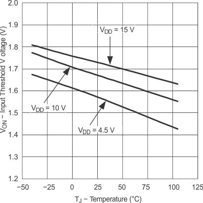
| VIN_H | Logic 1 input threshold | 2 | 2 | V | |||||||
| VIN_L | Logic 0 input threshold | 1 | 1 | V | |||||||
| Input current | 0 V ≤ VIN ≤ VDD | –10 | 0 | 10 | –10 | 0 | 10 | μA | |||
| OUTPUT (OUTA, OUTB) | |||||||||||
| Output current | VDD = 14 V(1)(2) | 4 | 4 | A | |||||||
| VOH | High-level output voltage | VOH = VDD – VOUT, IOUT = –10 mA | 330 | 450 | 330 | 450 | mV | ||||
| VOL | Low-level output level | IOUT = 10 mA | 22 | 40 | 22 | 40 | mV | ||||
| Output resistance high | IOUT = –10 mA, VDD = 14 V(3) | TA = 25°C | 25 | 30 | 35 | 25 | 30 | 35 | Ω | ||
| TA = full range | 14 | 45 | 18 | 45 | |||||||
| Output resistance low | IOUT = –10 mA, VDD = 14 V(3) | TA = 25°C | 1.9 | 2.2 | 2.5 | 1.9 | 2.2 | 2.5 | Ω | ||
| TA = full range | 0.95 | 4 | 1.2 | 4 | |||||||
| Latch-up protection(1) | 500 | 500 | mA | ||||||||
| SWITCHING TIME | |||||||||||
| tR | Rise time (OUTA, OUTB) | CLOAD = 1.8 nF(1) | 20 | 40 | 20 | 40 | ns | ||||
| tF | Fall time (OUTA, OUTB) | CLOAD = 1.8 nF(1) | 15 | 40 | 15 | 40 | ns | ||||
| tD1 | Delay, IN rising (IN to OUT) | CLOAD = 1.8 nF(1) | 35 | 55 | 35 | 50 | ns | ||||
| tD2 | Delay, IN falling (IN to OUT) | CLOAD = 1.8 nF(1) | 25 | 60 | 25 | 45 | ns | ||||
| ENABLE (ENBA, ENBB) | |||||||||||
| VIN_H | High-level input voltage | Low-to-high transition | 1.7 | 2.4 | 3.1 | 1.7 | 2.4 | 2.9 | V | ||
| VIN_L | Low-level input voltage | High-to-low transition | 1.1 | 1.8 | 2.3 | 1.1 | 1.8 | 2.2 | V | ||
| Hysteresis | 0.13 | 0.55 | 1.1 | .10 | 0.55 | 0.9 | V | ||||
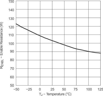
| RENBL | Enable impedance | VDD = 14 V, | ENBL = GND | 75 | 100 | 160 | 75 | 100 | 140 | kΩ | |
| tD3 | Propagation delay time(4) | CLOAD = 1.8 nF(1) | 30 | 60 | 30 | 60 | ns | ||||
| tD4 | Propagation delay time(4) | CLOAD = 1.8 nF(1) | 100 | 150 | 100 | 150 | ns | ||||
| OVERALL | |||||||||||
| IDD | Static operating current, VDD = 15 V, ENBA = ENBB = 15 V |
INA = 0 V | INB = 0 V | 900 | 1350 | 300 | 450 | μA | |||
| INB = High | 750 | 1100 | 750 | 1100 | |||||||
| INA = HIGH | INB = 0 V | 750 | 1100 | 750 | 1100 | ||||||
| INB = High | 600 | 900 | 1200 | 1800 | |||||||
| Disabled, VDD = 15 V, ENBA = ENBB = 0 V |
INA = 0 V | INB = 0 V | 300 | 450 | 300 | 450 | |||||
| INA = High | 450 | 700 | 450 | 700 | |||||||
| INA = HIGH | INB = 0 V | 450 | 700 | 450 | 700 | ||||||
| INB = High | 600 | 900 | 600 | 900 | |||||||
(1) Specified by design. Not tested in production.
(2) The pullup/pulldown circuits of the driver are bipolar and MOSFET transistors in parallel. The pulsed output current rating is the combined current from the bipolar and MOSFET transistors.
(3) The pullup/pulldown circuits of the driver are bipolar and MOSFET transistors in parallel. The output resistance is the RDS(ON) of the MOSFET transistor when the voltage on the driver output is less than the saturation voltage of the bipolar transistor.
(4) See Figure 2.
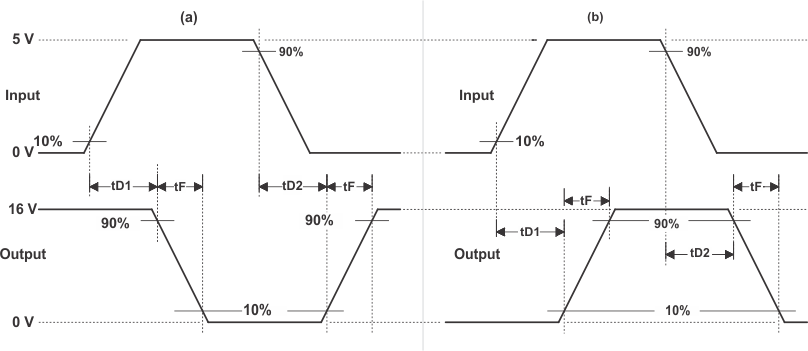
A. The 10% and 90% thresholds depict the dynamics of the bipolar output devices that dominate the power MOSFET transition through the Miller regions of operation.
Figure 1. Switching Waveforms for (a) Inverting Driver and (b) Noninverting Driver
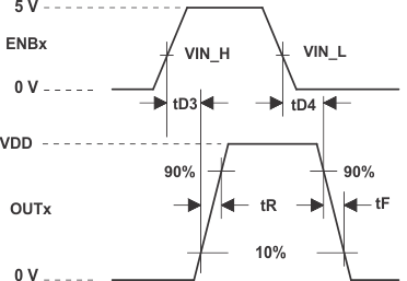
A. The 10% and 90% thresholds depict the dynamics of the bipolar output devices that dominate the power MOSFET transition through the Miller regions of operation.
Figure 2. Switching Waveform for Enable to Output
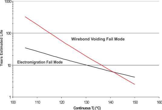
A. See data sheet for absolute maximum and minimum recommended operating conditions.
B. Silicon operating life design goal is 10 years at 105°C junction temperature (does not include package interconnect life).
C. Enhanced plastic product disclaimer applies
Figure 3. UCC27424MDGNREP Operating Life Derating Chart
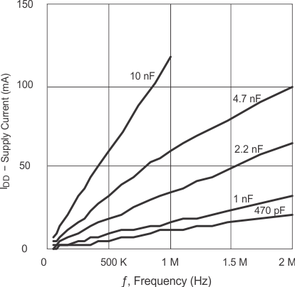
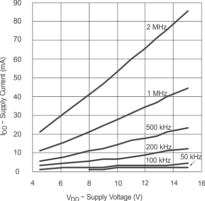
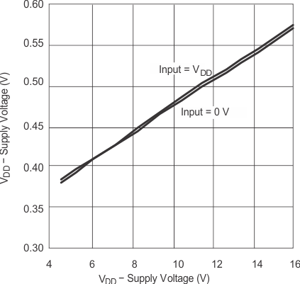
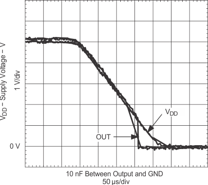
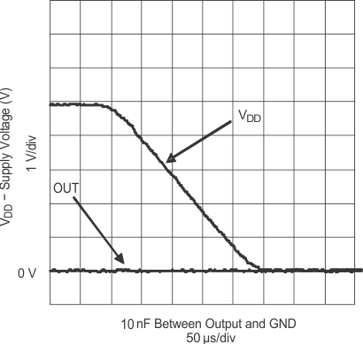
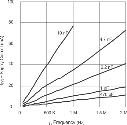
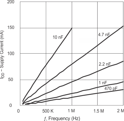
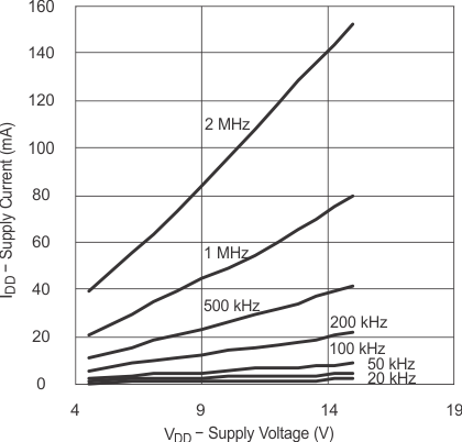
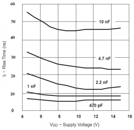
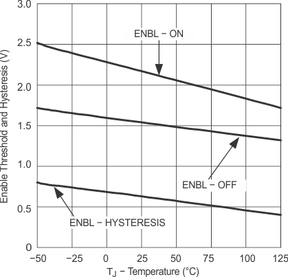
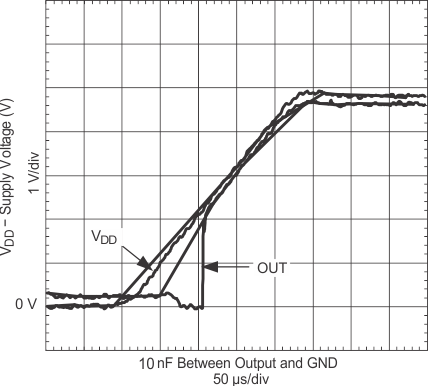
6.7 Typical Characteristics
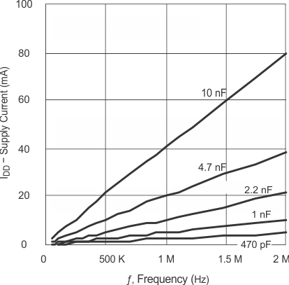
(CLOAD = 2.2 nF)
| IN = GND | ENBL = VDD | |
| IN = VDD | ENBL = VDD | |
| IN = VDD | ENBL = VDD | |
| IN = GND | ENBL = VDD | |
(CLOAD = 4.7 nF)
| IN = GND | ENBL = VDD | |
| IN = VDD | ENBL = VDD | |
| IN = VDD | ENBL = VDD | |
| IN = GND | ENBL = VDD | |