SLUSD95A March 2018 – January 2024 UCC27511A
PRODUCTION DATA
- 1
- 1 Features
- 2 Applications
- 3 Description
- 4 Pin Configuration and Functions
- 5 Specifications
- 6 Detailed Description
- 7 Application and Implementation
- 8 Power Supply Recommendations
- 9 Layout
- 10Device and Documentation Support
- 11Revision History
- 12Mechanical, Packaging, and Orderable Information
Package Options
Mechanical Data (Package|Pins)
- DBV|6
Thermal pad, mechanical data (Package|Pins)
Orderable Information
3 Description
The UCC27511A device is a compact gate driver that offers superior replacement of NPN and PNP discrete driver (buffer circuit) solutions. The UCC27511A device is a single-channel low-side, high-speed gate driver rated for MOSFETs, IGBTs, and emerging wide-bandgap power devices such as GaN. The device features fast rise times, fall times, and propagation delays, making the UCC27511A device suitable for high-speed applications. Its asymmetrical 4A peak source and 8A peak sink currents boost immunity against parasitic Miller turnon effect. The split output configuration enables easy and independent adjustment of rise and fall times using only two resistors and eliminating the need for an external diode. Features including wide input hysteresis and negative input voltage handling enhance transient immunity.
| PART NUMBER | PACKAGE(1) | BODY SIZE (NOM) |
|---|---|---|
| UCC27511A | DBV (SOT-23 6) | 2.90mm × 1.60mm |
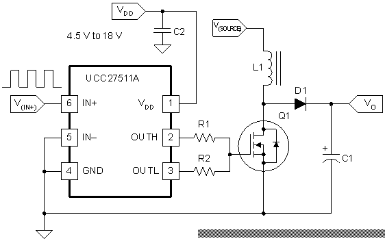
 Non-Inverting Input Application Diagram
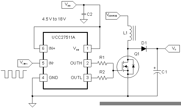
 Inverting Input Application Diagram