SLUSD95A March   2018  – January 2024 UCC27511A

PRODUCTION DATA  

  1.   1
  2. Features
  3. Applications
  4. Description
  5. Pin Configuration and Functions
  6. Specifications
    1. 5.1 Absolute Maximum Ratings
    2. 5.2 Handling Ratings
    3. 5.3 Recommended Operating Conditions
    4. 5.4 Thermal Information
    5. 5.5 Electrical Characteristics
    6. 5.6 Switching Characteristics
    7. 5.7 Typical Characteristics
  7. Detailed Description
    1. 6.1 Overview
    2. 6.2 Functional Block Diagram
    3. 6.3 Feature Description
      1. 6.3.1 VDD and Undervoltage Lockout
      2. 6.3.2 Operating Supply Current
      3. 6.3.3 Input Stage
      4. 6.3.4 Enable Function
      5. 6.3.5 Output Stage
      6. 6.3.6 Low Propagation Delays
    4. 6.4 Device Functional Modes
  8. Application and Implementation
    1. 7.1 Application Information
    2. 7.2 Typical Application
      1. 7.2.1 Design Requirements
      2. 7.2.2 Detailed Design Procedure
        1. 7.2.2.1 Input-to-Output Logic
        2. 7.2.2.2 Input Threshold Type
        3. 7.2.2.3 VDD Bias Supply Voltage
        4. 7.2.2.4 Peak Source and Sink Currents
        5. 7.2.2.5 Enable and Disable Function
        6. 7.2.2.6 Propagation Delay
        7. 7.2.2.7 Thermal Information
        8. 7.2.2.8 Power Dissipation
      3. 7.2.3 Application Curves
  9. Power Supply Recommendations
  10. Layout
    1. 9.1 Layout Guidelines
    2. 9.2 Layout Example
  11. 10Device and Documentation Support
    1. 10.1 Device Support
      1. 10.1.1 Third-Party Products Disclaimer
    2. 10.2 Receiving Notification of Documentation Updates
    3. 10.3 Support Resources
    4. 10.4 Trademarks
    5. 10.5 Electrostatic Discharge Caution
    6. 10.6 Glossary
  12. 11Revision History
  13. 12Mechanical, Packaging, and Orderable Information

Package Options

Mechanical Data (Package|Pins)
Thermal pad, mechanical data (Package|Pins)
Orderable Information

Typical Characteristics

GUID-7F554D27-4AE5-4AED-9CE0-1CDB00B08FD9-low.gif
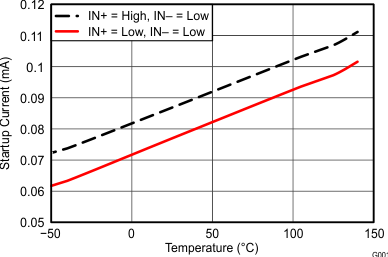
VDD = 3.4 V
Figure 5-5 Startup Current vs Temperature
GUID-C063B23F-3F45-460D-863D-2DF856B8878E-low.gif
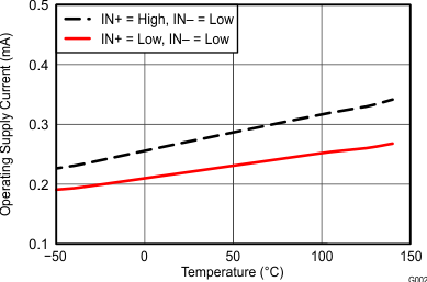
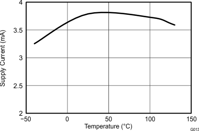
VDD = 12 V
Figure 5-7 Supply Current vs Temperature (Output in DC On or Off Condition)
GUID-86FCEA04-2295-4CCE-8767-3D9E627B56D0-low.gif
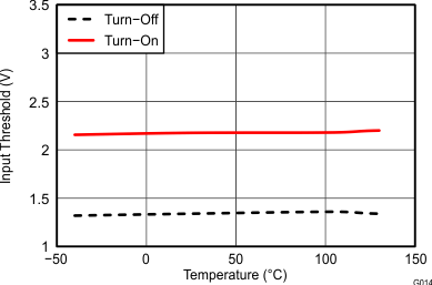
VDD = 12 VC(LOAD) = 1.8 nF
Figure 5-9 Input Threshold vs Temperature
GUID-DF6CCC8E-C47A-44BE-946C-9374C57990A2-low.gif
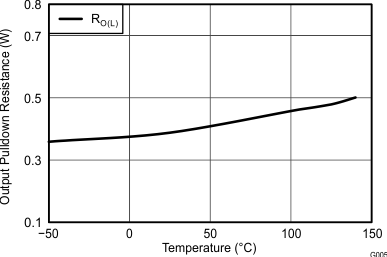
VDD = 12 VIO = 10 mA
Figure 5-11 Output Pull-Down Resistance vs Temperature
GUID-9014507D-3AB8-4B77-9F82-1DBEC9F159CC-low.gif
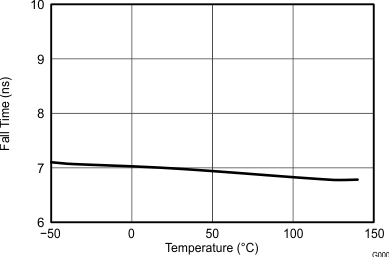
VDD = 12 VC(LOAD) = 1.8 nF
Figure 5-13 Fall Time vs Temperature
GUID-DCE808F4-71F5-4610-9BA0-DFBA1314D9F2-low.gif
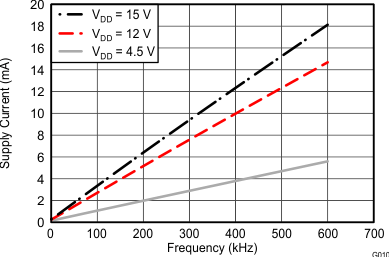
C(LOAD) = 1.8 nF
Figure 5-15 Operating Supply Current vs Frequency
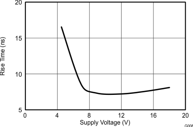
GUID-C81AC075-32C8-4431-85B5-5C60BEB6EF21-low.gif
Figure 5-17 Rise Time vs Supply Voltage
GUID-B88B81C7-70D2-422D-ADD8-F9DE6469EF4D-low.gif
VDD = 12 VC(LOAD) = 500 pFƒS = 500 kHz
Figure 5-6 Operating Supply Current vs Temperature (Output Switching)
GUID-86FC4A8F-4799-4234-9B25-E625009FFD53-low.gif
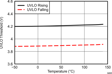
Figure 5-8 UVLO Threshold Voltage vs Temperature
GUID-DF8D6F87-BDA8-4757-84AF-427434CC3C94-low.gif
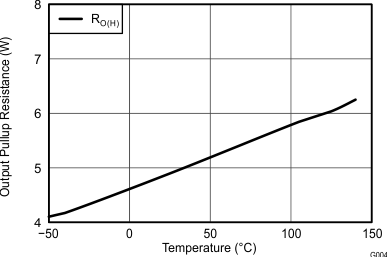
VDD = 12 VIO = 10 mA
Figure 5-10 Output Pullup Resistance vs Temperature
GUID-0DEEABC1-2B83-4CB7-B781-8B7DD1652AB9-low.gif
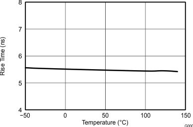
VDD = 12 VC(LOAD) = 1.8 nF
Figure 5-12 Rise Time vs Temperature
GUID-8BED6709-DFC5-4812-B3EC-6B4F202AC89B-low.gif
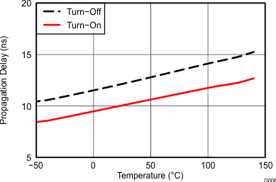
VDD = 12 V
Figure 5-14 Input to Output Propagation Delay vs Temperature
GUID-DD27184A-9279-4234-A1C7-A7AE9D0C7B94-low.gif
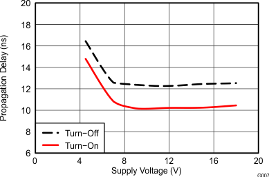
Figure 5-16 Propagation Delays vs Supply Voltage
GUID-CE96DE8C-7EFF-4BEB-A410-BD30623D4B31-low.gif
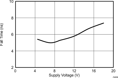
Figure 5-18 Fall Time vs Supply Voltage