SLUSB33A May 2012 – December 2014 UCC27518 , UCC27519
PRODUCTION DATA.
- 1 Features
- 2 Applications
- 3 Description
- 4 Revision History
- 5 Description (continued)
- 6 Device Comparison Table
- 7 Pin Configuration and Functions
- 8 Specifications
- 9 Detailed Description
- 10Application and Implementation
- 11Power Supply Recommendations
- 12Layout
- 13Device and Documentation Support
- 14Mechanical, Packaging, and Orderable Information
Package Options
Mechanical Data (Package|Pins)
- DBV|5
Thermal pad, mechanical data (Package|Pins)
Orderable Information
10 Application and Implementation
NOTE
Information in the following applications sections is not part of the TI component specification, and TI does not warrant its accuracy or completeness. TI’s customers are responsible for determining suitability of components for their purposes. Customers should validate and test their design implementation to confirm system functionality.
10.1 Application Information
High-current gate driver devices are required in switching power applications for a variety of reasons. In order to effect fast switching of power devices and reduce associated switching power losses, a powerful gate driver can be employed between the PWM output of controllers and the gates of the power semiconductor devices. Gate drivers also find other needs such as minimizing the effect of high-frequency switching noise by locating the high-current driver physically close to the power switch, driving gate-drive transformers and controlling floating power-device gates, reducing power dissipation and thermal stress in controllers by moving gate charge power losses into itself. Finally, emerging wide band-gap power device technologies such as GaN based switches, which are capable of supporting very high switching frequency operation, are driving very special requirements in terms of gate drive capability. These requirements include operation at low VDD voltages (5 V or lower), low propagation delays and availability in compact, low-inductance packages with good thermal capability. In summary gate-driver devices are extremely important components in switching power combining benefits of high-performance, low cost, component count and board space reduction and simplified system design.
10.2 Typical Application
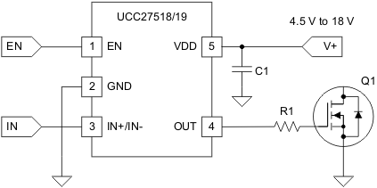 Figure 23. Typical Application Diagram
10.2.1 Design Requirements
When selecting the proper gate driver device for an end application, some design considerations must be evaluated first to make the most appropriate selection. Among these considerations are input-to-output configuration, the input threshold type, bias supply voltage levels, peak source and sink currents, availability of independent enable and disable functions, propagation delay, power dissipation, and package type.
Table 4. Design Parameters
| Design Parameter | Example Value |
|---|---|
| Input-to-Output Logic | Noninverting |
| Input Threshold Type | CMOS type |
| VDD Bias Supply Voltage | 10 V (Minimum), 13 V (Nominal), 15 V (Peak) |
| Peak Source and Sink Currents | Minimum 3 A Source, Minimum 3 A Sink |
| Enable and Disable Function | Yes, Needed |
| Propagation Delay | Maximum 40 ns or less |
10.2.2 Detailed Design Procedure
10.2.2.1 Input-to-Output Logic
The design must specify which type of input-to-output configuration should be used. If turning on the power MOSFET or IGBT when the input signal is in high state is preferred, then the noninverting configuration must be selected. If turning off the power MOSFET or IGBT when the input signal is in high state is preferred, the inverting configuration must be chosen. The UCC27518 and UCC27519 devices follow inverting and noninverting logic, respectively.
10.2.2.2 Input Threshold Type
The type of input voltage threshold determines the type of controller used with the gate driver device. The UCC27518 and UCC27519 devices feature CMOS input threshold logic, with wide hysteresis. In CMOS input threshold logic, the threshold voltage level is a function of the bias voltage on the VDD pin of the device. The typical high threshold is 55% of VDD supply voltage, and the typical low threshold is 39% of VDD supply voltage at VDD=12V. There is built-in hysteresis, which is typically 16% of VDD supply voltage. See Electrical Characteristics for the actual input threshold voltage levels and hysteresis specifications for the UCC27518 and UCC27519 devices at different VDD bias levels.
In most applications, the absolute value of the threshold voltage offered by the CMOS logic will be higher (eg.VINH = 5.5 V if VDD = 10 V) than what is offered by logic level threshold devices. This offers the following benefits:
- Better noise immunity due to the higher threshold level desirable in high power systems.
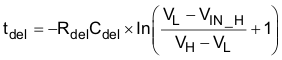
- Ability to accept slow dV/dt input signals, which allows designers to use RCD circuits on the input pin to program propagation delays in the application, as shown in Figure 24.
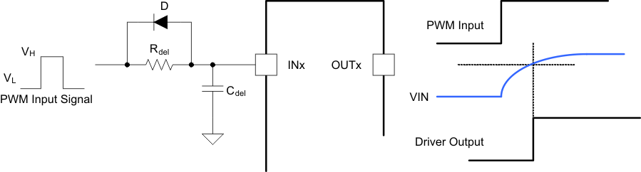 Figure 24. Using RCD Circuits
As a result of the CMOS input logic, the UCC27518 and UCC27519 devices cannot be driven directly by logic level control signals from microcontrollers, digital power controllers, or DSPs. The UCC27518 and UCC27519 are ideally suited for being driven by analog controllers driven by the same VDD voltage as the gate driver devices.
10.2.2.3 VDD Bias Supply Voltage
The bias supply voltage to be applied to the VDD pin of the device should never exceed the values listed in Recommended Operating Conditions. However, different power switches demand different voltage levels to be applied at the gate terminals for effective turn on and turnoff. With certain power switches, a positive gate voltage may be required for turn on, and a negative gate voltage may be required for turnoff, in which case the VDD bias supply equals the voltage differential. With a wide operating range from 4.5 V to 18 V, the UCC27518 and UCC27519 devices can be used to drive a variety of power switches, such as Si MOSFETs (for example, VGS = 4.5 V, 10 V, 12 V), IGBTs (VGE = 15 V, 18 V), and wide-band gap power semiconductors (such as GaN, certain types of which allow no higher than 6 V to be applied to the gate terminals).
10.2.2.4 Peak Source and Sink Currents
Generally, the switching speed of the power switch during turn on and turnoff should be as fast as possible, to minimize switching power losses. The gate driver device must be able to provide the required peak current for achieving the targeted switching speeds for the targeted power MOSFET. Using the example of a power MOSFET, the system requirement for the switching speed is typically described in terms of the slew rate of the drain-to-source voltage of the power MOSFET (such as dVDS/dt).
For example, the system requirement might state that a SPP20N60C3 power MOSFET must be turned-on with a dVDS/dt of 20V/ns or higher under a DC bus voltage of 400 V in a continuous-conduction-mode (CCM) boost PFC-converter application. This type of application is an inductive, hard-switching application, and reducing switching power losses is critical. This requirement means that the entire drain-to-source voltage swing during power MOSFET turnon event (from 400 V in the OFF state to VDS(on) in on state) must be completed in approximately 20 ns or less.
When the drain-to-source voltage swing occurs, the Miller charge of the power MOSFET (QGD parameter in SPP20N60C3 power MOSFET data sheet = 33 nC typical) is supplied by the peak current of gate driver. According to the power MOSFET inductive switching mechanism, the gate-to-source voltage of the power MOSFET at this time is the Miller plateau voltage, which is typically a few volts higher than the threshold voltage of the power MOSFET, VGS(TH). To achieve the targeted dVDS/dt, the gate driver must be capable of providing the QGD charge in 20 ns or less. In other words, a peak current of 1.65 A (= 33 nC / 20 ns) or higher must be provided by the gate driver. The UCC27518 and UCC27519 gate driver is capable of providing 4-A peak sourcing current, which exceeds the design requirement and has the capability to meet the necessary switching speed.
The 2.4x overdrive capability provides an extra margin against part-to-part variations in the QGD parameter of the power MOSFET, along with additional flexibility to insert external gate resistors and fine tune the switching speed for efficiency versus EMI optimizations. However, in practical designs the parasitic trace inductance in the gate drive circuit of the PCB will have a definitive role to play on the power MOSFET switching speed. The effect of this trace inductance is to limit the dI/dt of the output current pulse of the gate driver.
To illustrate this, consider the output current pulse waveform from the gate driver to be approximated to a triangular profile, where the area under the triangle (½ ×IPEAK × time) would equal the total gate charge of the power MOSFET (QG parameter in SPP20N60C3 power MOSFET datasheet = 87 nC typical). If the parasitic trace inductance limits the dI/dt, the full peak current capability of the gate driver may not be fully achieved in the time required to deliver the QG required for the power MOSFET switching. In other words, the time parameter in the equation would dominate and the IPEAK value of the current pulse would be much less than the true peak current capability of the device, while the required QG is still delivered. Because of this, the desired switching speed may not be realized, even when theoretical calculations indicate the gate driver is capable of achieving the targeted switching speed. Thus, place the gate driver device very close to the power MOSFET and design a tight gate drive-loop with minimal PCB trace inductance to realize the full peak-current capability of the gate driver.
10.2.2.5 Enable and Disable Function
Certain applications demand independent control of the output state of the driver without involving the input signal. The UCC27518 and UCC27519 devices offer the Enable pin, which achieves this.
10.2.2.6 Propagation Delay
The acceptable propagation delay from the gate driver is dependent on the switching frequency at which it is used, and the acceptable level of pulse distortion to the system. The UCC27518 and UCC27519 devices feature industry best-in-class 17-ns (typical) propagation delays, which ensure very little pulse distortion and allow operation at very high-frequencies. See Switching Characteristics for the propagation and switching characteristics of the UCC27518 and UCC27519 devices.
10.2.3 Application Curve
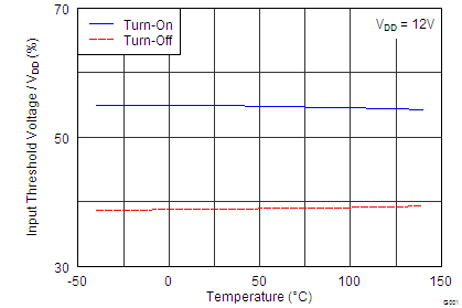 Figure 25. Input Threshold vs Temperature