SLUSB33A May 2012 – December 2014 UCC27518 , UCC27519
PRODUCTION DATA.
- 1 Features
- 2 Applications
- 3 Description
- 4 Revision History
- 5 Description (continued)
- 6 Device Comparison Table
- 7 Pin Configuration and Functions
- 8 Specifications
- 9 Detailed Description
- 10Application and Implementation
- 11Power Supply Recommendations
- 12Layout
- 13Device and Documentation Support
- 14Mechanical, Packaging, and Orderable Information
Package Options
Mechanical Data (Package|Pins)
- DBV|5
Thermal pad, mechanical data (Package|Pins)
Orderable Information
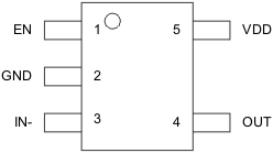
7 Pin Configuration and Functions
UCC27518
SOT-23 DBV
(Top View)
UCC27519
SOT-23 DBV
(Top View)
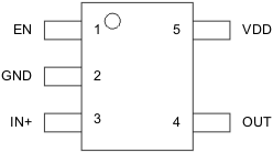
Pin Functions
| PIN | I/O | DESCRIPTION | |
|---|---|---|---|
| NO. | NAME | ||
| 1 | EN | I | Enable input: (EN biased LOW disables output regardless of Input state, EN biased high or floating enables output, EN is allowed to float hence it is pin-to-pin compatible with TPS282X N/C pin) |
| 2 | GND | — | Ground: All signals referenced to this pin |
| 3 | IN– | I | Input: Inverting input in the UCC27518, output held LOW if IN– is unbiased or floating |
| IN+ | I | Input: Noninverting input in the UCC27519, output held LOW if IN+ is unbiased or floating | |
| 4 | OUT | O | Sourcing and sinking current output of driver |
| 5 | VDD | I | Supply input |