SLUSBA5F December 2012 – March 2018 UCC27611
PRODUCTION DATA.
- 1 Features
- 2 Applications
- 3 Description
- 4 Revision History
- 5 Pin Configuration and Functions
- 6 Specifications
- 7 Detailed Description
- 8 Application and Implementation
- 9 Power Supply Recommendations
- 10Layout
- 11Device and Documentation Support
- 12Mechanical, Packaging, and Orderable Information
Package Options
Mechanical Data (Package|Pins)
- DRV|6
Thermal pad, mechanical data (Package|Pins)
- DRV|6
Orderable Information
8.2.2.3 Output Configuration
Generally, the switching speed of the power switch during turnon and turnoff must be as fast as possible to minimize switching power losses. The gate driver device must be able to provide the required peak current for achieving the targeted switching speeds for the targeted power MOSFET. In practical designs, the parasitic trace inductance in the gate drive circuit of the PCB has a definitive role to play on the power MOSFET switching speed. The effect of this trace inductance is to limit the dI/dt of the output current pulse of the gate driver. Because of this, the desired switching speed may not be realized, even when theoretical calculations indicate the gate driver can achieve the targeted switching speed. Thus, placing the gate driver device very close to the power MOSFET and designing a tight gate drive-loop with minimal PCB trace inductance is important to realize the full peak-current capability of the gate driver.
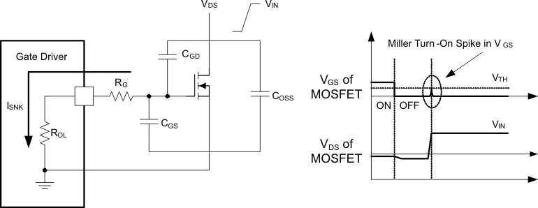
The UCC27611 is capable of delivering 4-A source, 6-A sink (asymmetrical drive) at VDD = 12 V. Strong sink capability in asymmetrical drive results in a very low pulldown impedance in the driver output stage which boosts immunity against parasitic, Miller turnon (C × dV/dt turnon) effect, especially where low gate-charge MOSFETs or emerging wide band-gap GaN power switches are used.
An example of a situation where Miller turnon is a concern is synchronous rectification (SR). In SR application, the dV/dt occurs on MOSFET drain when the MOSFET is already held in OFF state by the gate driver. The current discharging the CGD Miller capacitance during this dV/dt is shunted by the pulldown stage of the driver. If the pulldown impedance is not low enough, then a voltage spike can result in the VGS of the MOSFET, which can result in spurious turnon. This phenomenon is illustrated in Figure 13. UCC27611 offers a best-in-class, 0.35-Ω (typ) pulldown impedance boosting immunity against Miller turnon.

If limiting the rise or fall times to the power device to reduce EMI is necessary, then an external resistance is highly recommended between the output of the driver and the power device. This external resistor has the additional benefit of reducing part of the gate charge related power dissipation in the gate driver device package and transferring it into the external resistor itself. The split outputs of the UCC27611 offer flexibility to adjust the turnon and turnoff speed independently by adding additional impedance in either the turnon path (OUTH) and/or turnoff path (OUTL).