SLUSCR9B June 2017 – December 2020 UCC28730-Q1
PRODUCTION DATA
- 1 Features
- 2 Applications
- 3 Description
- 4 Revision History
- 5 Pin Configuration and Functions
- 6 Specifications
-
7 Detailed Description
- 7.1 Overview
- 7.2 Functional Block Diagram
- 7.3 Feature Description
- 7.4 Device Functional Modes
-
8 Application and Implementation
- 8.1 Application Information
- 8.2
Typical Application
- 8.2.1 Design Requirements
- 8.2.2
Detailed Design Procedure
- 8.2.2.1 Stand-By Power Estimate
- 8.2.2.2 Input Bulk Capacitance and Minimum Bulk Voltage
- 8.2.2.3 Transformer Turns Ratio, Inductance, Primary-Peak Current
- 8.2.2.4 Transformer Parameter Verification
- 8.2.2.5 Output Capacitance
- 8.2.2.6 VDD Capacitance, CVDD
- 8.2.2.7 VS Resistor Divider, Line Compensation, and Cable Compensation
- 8.2.2.8 VS Wake-Up Detection
- 8.2.3 Application Curves
- 8.3 Do's and Don'ts
- 9 Power Supply Recommendations
- 10Layout
-
11Device and Documentation Support
- 11.1
Device Support
- 11.1.1
Device Nomenclature
- 11.1.1.1 Capacitance Terms in Farads
- 11.1.1.2 Duty-Cycle Terms
- 11.1.1.3 Frequency Terms in Hertz
- 11.1.1.4 Current Terms in Amperes
- 11.1.1.5 Current and Voltage Scaling Terms
- 11.1.1.6 Transformer Terms
- 11.1.1.7 Power Terms in Watts
- 11.1.1.8 Resistance Terms in Ω
- 11.1.1.9 Timing Terms in Seconds
- 11.1.1.10 DC Voltage Terms in Volts
- 11.1.1.11 AC Voltage Terms in Volts
- 11.1.1.12 Efficiency Terms
- 11.1.1
Device Nomenclature
- 11.2 Documentation Support
- 11.3 Receiving Notification of Documentation Updates
- 11.4 Support Resources
- 11.5 Trademarks
- 11.6 Electrostatic Discharge Caution
- 11.7 Glossary
- 11.1
Device Support
- 12Mechanical, Packaging, and Orderable Information
Package Options
Mechanical Data (Package|Pins)
- D|7
Thermal pad, mechanical data (Package|Pins)
Orderable Information
7.3.4 Primary-Side Constant Current Regulation
Timing information at the VS pin and current information at the CS pin allow accurate regulation of the secondary average current. The control law dictates that as power is increased in CV regulation and approaching CC regulation the primary-peak current will be at IPP(max). Referring to Figure 7-5 below, the primary-peak current, turns ratio, secondary demagnetization time (tDM), and switching period (tSW) determine the secondary average output current. Ignoring leakage inductance effects, the average output current is given by Equation 6.
 Figure 7-5 Transformer Currents Relationship
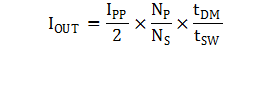
When the average output current reaches the CC regulation reference in the current control block, the controller operates in frequency modulation mode to control the output current, IOCC, at any output voltage down to or below the minimum operating voltage target, VOCC (as seen in Figure 7-6), as long as the auxiliary winding can keep VDD voltage above the UVLO turn-off threshold. When VO falls so low that VDD cannot be sustained above UVLO, the device shuts down.
 Figure 7-6 Typical Output V-I Target Characteristic