SLUSCR9B June 2017 – December 2020 UCC28730-Q1
PRODUCTION DATA
- 1 Features
- 2 Applications
- 3 Description
- 4 Revision History
- 5 Pin Configuration and Functions
- 6 Specifications
-
7 Detailed Description
- 7.1 Overview
- 7.2 Functional Block Diagram
- 7.3 Feature Description
- 7.4 Device Functional Modes
-
8 Application and Implementation
- 8.1 Application Information
- 8.2
Typical Application
- 8.2.1 Design Requirements
- 8.2.2
Detailed Design Procedure
- 8.2.2.1 Stand-By Power Estimate
- 8.2.2.2 Input Bulk Capacitance and Minimum Bulk Voltage
- 8.2.2.3 Transformer Turns Ratio, Inductance, Primary-Peak Current
- 8.2.2.4 Transformer Parameter Verification
- 8.2.2.5 Output Capacitance
- 8.2.2.6 VDD Capacitance, CVDD
- 8.2.2.7 VS Resistor Divider, Line Compensation, and Cable Compensation
- 8.2.2.8 VS Wake-Up Detection
- 8.2.3 Application Curves
- 8.3 Do's and Don'ts
- 9 Power Supply Recommendations
- 10Layout
-
11Device and Documentation Support
- 11.1
Device Support
- 11.1.1
Device Nomenclature
- 11.1.1.1 Capacitance Terms in Farads
- 11.1.1.2 Duty-Cycle Terms
- 11.1.1.3 Frequency Terms in Hertz
- 11.1.1.4 Current Terms in Amperes
- 11.1.1.5 Current and Voltage Scaling Terms
- 11.1.1.6 Transformer Terms
- 11.1.1.7 Power Terms in Watts
- 11.1.1.8 Resistance Terms in Ω
- 11.1.1.9 Timing Terms in Seconds
- 11.1.1.10 DC Voltage Terms in Volts
- 11.1.1.11 AC Voltage Terms in Volts
- 11.1.1.12 Efficiency Terms
- 11.1.1
Device Nomenclature
- 11.2 Documentation Support
- 11.3 Receiving Notification of Documentation Updates
- 11.4 Support Resources
- 11.5 Trademarks
- 11.6 Electrostatic Discharge Caution
- 11.7 Glossary
- 11.1
Device Support
- 12Mechanical, Packaging, and Orderable Information
Package Options
Mechanical Data (Package|Pins)
- D|7
Thermal pad, mechanical data (Package|Pins)
Orderable Information
7.3.1.7 CS (Current Sense)
The current-sense pin connects to a series resistor (RLC) to the current-sense resistor (RCS). The maximum current-sense threshold (VCST(max)) is approximately 0.74 V for IPP(max) and minimum current-sense threshold (VCST(min)) is approximately 0.25 V for IPP(min). RLC provides the function of feed-forward line compensation to eliminate changes in IPP with input voltage due to the propagation delay of the internal comparator and MOSFET turn-off time. An internal leading-edge blanking time of 225 ns eliminates sensitivity to the MOSFET turn-on current spike. It should not be necessary to place a bypass capacitor on the CS pin. The target output current in constant-current (CC) regulation determines the value of RCS. The values of RCS and RLC are calculated by Equation 4 and Equation 5. The term VCCR is the product of the demagnetization constant, 0.432, and VCST(max). VCCR is held to a tighter accuracy than either of its constituent terms. The term ηXFMR accounts for the energy stored in the transformer but not delivered to the secondary. This term includes transformer resistance and core loss, bias power, and primary-to-secondary leakage ratio.
Example: With a transformer core and winding loss of 5%, primary-to-secondary leakage inductance of 3.5%, and bias-power to output-power ratio of 0.5%, the ηXFMR value at full-power is: 1 - 0.05 - 0.035 - 0.005 = 0.91.

where
- VCCR is a constant-current regulation factor (see Section 6.5),
- NPS is the transformer primary-to-secondary turns-ratio, (a ratio of 13 to 15 is typical for a 5-V output),
- IOCC is the target output current in constant-current regulation,
- ηXFMR is the transformer efficiency at full-power output.
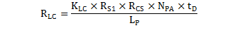
where
- KLC is a current-scaling constant for line compensation (see Section 6.5),
- RS1 is the VS pin high-side resistor value,
- RCS is the current-sense resistor value,
- NPA is the transformer primary-to-auxiliary turns-ratio,
- tD is the total current-sense delay consisting of MOSFET turn-off delay, plus approximately 50-ns internal delay,
- LP is the transformer primary inductance.