SLUSCR9B June 2017 – December 2020 UCC28730-Q1
PRODUCTION DATA
- 1 Features
- 2 Applications
- 3 Description
- 4 Revision History
- 5 Pin Configuration and Functions
- 6 Specifications
-
7 Detailed Description
- 7.1 Overview
- 7.2 Functional Block Diagram
- 7.3 Feature Description
- 7.4 Device Functional Modes
-
8 Application and Implementation
- 8.1 Application Information
- 8.2
Typical Application
- 8.2.1 Design Requirements
- 8.2.2
Detailed Design Procedure
- 8.2.2.1 Stand-By Power Estimate
- 8.2.2.2 Input Bulk Capacitance and Minimum Bulk Voltage
- 8.2.2.3 Transformer Turns Ratio, Inductance, Primary-Peak Current
- 8.2.2.4 Transformer Parameter Verification
- 8.2.2.5 Output Capacitance
- 8.2.2.6 VDD Capacitance, CVDD
- 8.2.2.7 VS Resistor Divider, Line Compensation, and Cable Compensation
- 8.2.2.8 VS Wake-Up Detection
- 8.2.3 Application Curves
- 8.3 Do's and Don'ts
- 9 Power Supply Recommendations
- 10Layout
-
11Device and Documentation Support
- 11.1
Device Support
- 11.1.1
Device Nomenclature
- 11.1.1.1 Capacitance Terms in Farads
- 11.1.1.2 Duty-Cycle Terms
- 11.1.1.3 Frequency Terms in Hertz
- 11.1.1.4 Current Terms in Amperes
- 11.1.1.5 Current and Voltage Scaling Terms
- 11.1.1.6 Transformer Terms
- 11.1.1.7 Power Terms in Watts
- 11.1.1.8 Resistance Terms in Ω
- 11.1.1.9 Timing Terms in Seconds
- 11.1.1.10 DC Voltage Terms in Volts
- 11.1.1.11 AC Voltage Terms in Volts
- 11.1.1.12 Efficiency Terms
- 11.1.1
Device Nomenclature
- 11.2 Documentation Support
- 11.3 Receiving Notification of Documentation Updates
- 11.4 Support Resources
- 11.5 Trademarks
- 11.6 Electrostatic Discharge Caution
- 11.7 Glossary
- 11.1
Device Support
- 12Mechanical, Packaging, and Orderable Information
Package Options
Mechanical Data (Package|Pins)
- D|7
Thermal pad, mechanical data (Package|Pins)
Orderable Information
8.2.2.5 Output Capacitance
With ordinary flyback converters, the output capacitance value is typically determined by the transient response requirement for a specific load step, ITRAN, sometimes from a no-load condition. For example, in some USB charger applications, there is requirement to maintain a transient minimum VO of 4.1 V with a load-step of 0 mA to 500 mA. Equation 20 below assumes that the switching frequency can be at the UCC28730-Q1 minimum of fSW(min).
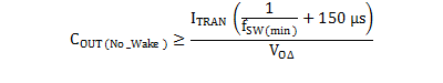
This results in a COUT value of over 17,000 µF, unless a substantial pre-load is used to raise the minimum switching frequency. However, the wake-up feature allows the use of a much smaller value for COUT because the wake-up response immediately cancels the Wait state and provides high-frequency power cycles to recover the output voltage from the load transient. The secondary-side voltage monitor UCC24650 provides the UCC28730-Q1 with a wake-up signal when it detects a -3% droop in output voltage.

where
- (dVOUT/dt) is the slope at which the UCC24650 must detect the VOUT droop. Use a slope factor of 3700 V/s or lower for this calculation.
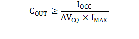
The UCC28730-Q1 incorporates internal voltage-loop compensation circuits so that external compensation is not necessary, provided that the value of COUT is high enough. The following equation determines a minimum value of COUT necessary to maintain a phase margin of about 40 degrees over the full-load range. KCo is a dimensionless factor which has a value of 100.

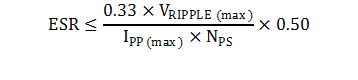
Another consideration for selecting the output capacitor(s) is the maximum ripple voltage requirement, VRIPPLE(max), which is reviewed based on the maximum output load, the secondary-peak current, and the equivalent series resistance (ESR) of the capacitor. The two major contributors to the output ripple voltage are the change in VOUT due to the charge and discharge of COUT between each switching cycle and the step in VOUT due to the ESR of COUT. TI recommends an initial allocation of 33% of VRIPPLE(max) to ESR, 33% to COUT, and the remaining 33% to account for additional low-level ripple from EMI-dithering, valley-hopping, sampling noise and other random contributors. In Equation 23, a margin of 50% is applied to the capacitor ESR requirement to allow for aging. In Equation 24, set ΔVCQ = 0.33 x VRIPPLE(max) to determine the minimum value of COUT with regard to ripple voltage limitation. If other allocations of the allowable ripple voltage are desired, these equations may be adjusted accordingly.
Choose the largest value of the previous COUT calculations for the minimum output capacitance. If the value of COUT becomes excessive to meet a stringent ripple limitation, a C-L-C pi-filter arrangement can be considered to as an alternative to a simple capacitor-only filter. This arrangement is beyond the scope of this datasheet.