JAJSGQ4G april 2010 – june 2023 DLPA200
PRODUCTION DATA
- 1
- 1 特長
- 2 アプリケーション
- 3 概要
- 4 Revision History
- 5 Device Configurations Table
- 6 Pin Configuration and Functions
-
7 Specifications
- 7.1 Absolute Maximum Ratings
- 7.2 ESD Ratings
- 7.3 Recommended Operating Conditions
- 7.4 Thermal Information
- 7.5 Electrical Characteristics Control Logic
- 7.6 5-V Linear Regulator
- 7.7 Bias Voltage Boost Converter
- 7.8 Reset Voltage Buck-Boost Converter
- 7.9 VOFFSET/DMDVCC2 Regulator
- 7.10 Switching Characteristics
- 8 Detailed Description
- 9 Application and Implementation
- 10Power Supply Recommendations
- 11Layout
- 12Device and Documentation Support
- 13Mechanical, Packaging, and Orderable Information
8.3.1 5-V Linear Regulator
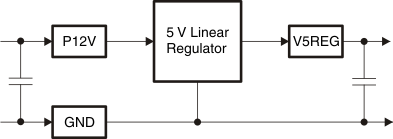
The 5-V linear regulator supplies the 5-V requirement of the DLPA200 internal logic.
Figure 8-1 shows the block diagram of this module. The input decoupling capacitors are shared with other internal DLPA200 modules. See Section 9.1.1 for recommended component values.
 Figure 8-1 5-Volt Linear Regulator Block Diagram