SLVSCE5B November 2013 – July 2016 DRV3203E-Q1
- 1 Features
- 2 Applications
- 3 Description
- 4 Revision History
- 5 Pin Configuration and Functions
- 6 Specifications
-
7 Detailed Description
- 7.1 Functional Block Diagram
- 7.2 Feature Description
- 7.3
Register Maps
- 7.3.1
Register Descriptions
- 7.3.1.1 CFGUNLK (address 0x01): Configuration Unlock Register
- 7.3.1.2 FLTCFG (address 0x02): Fault Detection Configuration Register
- 7.3.1.3 FLTEN0 (address 0x04): FAULT Pin Enable Register 0
- 7.3.1.4 FLTEN1 (address 0x05): FAULT Pin Enable Register 1
- 7.3.1.5 SDNEN0 (address 0x06): Pre-Driver Shutdown Enable Register 0
- 7.3.1.6 SDNEN1 (address 0x07): Pre-Driver Shutdown Enable Register 1
- 7.3.1.7 FLTFLG0 (address 0x08): Fault Flag Register 0
- 7.3.1.8 FLGFLT1 (address 0x09): Fault Flag Register 1
- 7.3.1.9 CSCFG (address 0x0A): Current Sense Configuration Register
- 7.3.1.10 PDCFG (address 0x0B): Pre-Driver Configuration Register
- 7.3.1.11 DIAG (address 0x0C): Diagnosis Register
- 7.3.1.12 SPARE (address 0x0D): Spare Register
- 7.3.1
Register Descriptions
- 8 Application and Implementation
- 9 Device and Documentation Support
- 10Mechanical, Packaging, and Orderable Information
8 Application and Implementation
NOTE
Information in the following applications sections is not part of the TI component specification, and TI does not warrant its accuracy or completeness. TI’s customers are responsible for determining suitability of components for their purposes. Customers should validate and test their design implementation to confirm system functionality.
8.1 Typical Application
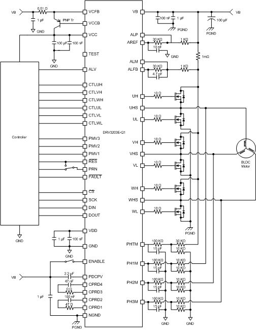
 Figure 27. Typical Application Schematic