SLVSCH0 April 2014 DRV8824-Q1
PRODUCTION DATA.
- 1 Features
- 2 Applications
- 3 Description
- 4 Simplified Schematic
- 5 Revision History
- 6 Terminal Configuration and Functions
- 7 Specifications
- 8 Detailed Description
- 9 Application and Implementation
- 10Power Supply Recommendations
- 11Layout
- 12Device and Documentation Support
- 13Mechanical, Packaging, and Orderable Information
パッケージ・オプション
メカニカル・データ(パッケージ|ピン)
- PWP|28
サーマルパッド・メカニカル・データ
- PWP|28
発注情報
9 Application and Implementation
9.1 Application Information
The DRV8824-Q1 is used in bipolar stepper control. The following design procedure can be used to configure the DRV8824-Q1.
9.2 Typical Application
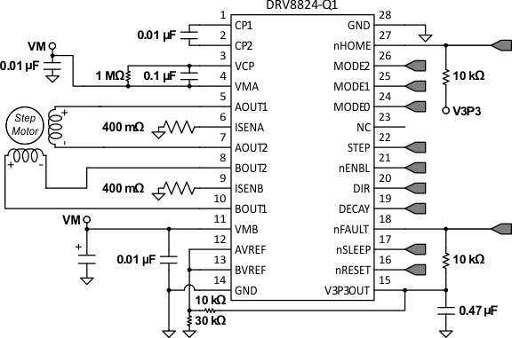 Figure 8. Typical Application Schematic
9.2.1 Design Requirements
Table 3 gives design input parameters for system design.
Table 3. Design Parameters
| DESIGN PARAMETER | REFERENCE | EXAMPLE VALUE |
|---|---|---|
| Supply voltage | VM | 24 V |
| Motor winding resistance | RL | 1.0 Ω/phase |
| Motor winding inductance | LL | 3.5 mH/phase |
| Motor full step angle | θstep | 1.8°/step |
| Target microstepping level | nm | 8 microsteps per step |
| Target motor speed | v | 120 rpm |
| Target full-scale current | IFS | 1.25 A |
9.2.2 Detailed Design Procedure
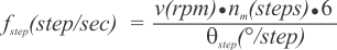
9.2.2.1 Stepper Motor Speed
The first step in configuring the DRV8824-Q1 requires the desired motor speed and microstepping level. If the target application requires a constant speed, then a square wave with frequency fstep must be applied to the STEP pin.
If the target motor speed is too high, the motor will not spin. Make sure that the motor can support the target speed.
For a desired motor speed (v), microstepping level (nm), and motor full step angle (θstep),
θstep can be found in the stepper motor datasheet or written on the motor itself.
For the DRV8824-Q1, the microstepping level is set by the USM pins and can be any of the settings in . Higher microstepping will mean a smother motor motion and less audible noise, but will increase switching losses and require a higher fstep to achieve the same motor speed.
9.2.2.2 Current Regulation
In a stepper motor, the full-scale current (IFS) is the maximum current driven through either winding. This quantity will depend on the VREF analog voltage and the sense resistor value (RSENSE). During stepping, IFS defines the current chopping threshold (ITRIP) for the maximum current step.
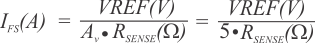
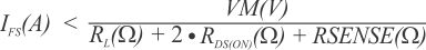
IFS is set by a comparator which compares the voltage across RSENSE to a reference voltage. There is a current sense amplifier built in with programmable gain through ISGAIN. Note that IFS must also follow the equation below in order to avoid saturating the motor. VM is the motor supply voltage and RL is the motor winding resistance.
9.2.2.3 Decay Modes
The DRV8824-Q1 supports three different decay modes: slow decay, fast decay, and mixed decay. The current through the motor windings is regulated using a fixed-frequency PWM scheme. This means that after any drive phase, when a motor winding current has hit the current chopping threshold (ITRIP), the DRV8824-Q1 will place the winding in one of the three decay modes until the PWM cycle has expired. Afterwards, a new drive phase starts.
The blanking time tBLANK defines the minimum drive time for the current chopping. ITRIP is ignored during tBLANK, so the winding current may overshoot the trip level.
9.2.3 Application Curves
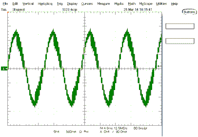 Figure 9. Microstepping Waveform, Phase A, Mixed Decay
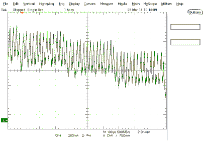 Figure 11. Microstepping Waveform, Mixed Decay on Decreasing Steps
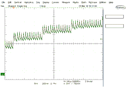 Figure 10. Microstepping Waveform, Slow Decay on Increasing Steps