SLVSCH0 April 2014 DRV8824-Q1
PRODUCTION DATA.
- 1 Features
- 2 Applications
- 3 Description
- 4 Simplified Schematic
- 5 Revision History
- 6 Terminal Configuration and Functions
- 7 Specifications
- 8 Detailed Description
- 9 Application and Implementation
- 10Power Supply Recommendations
- 11Layout
- 12Device and Documentation Support
- 13Mechanical, Packaging, and Orderable Information
パッケージ・オプション
メカニカル・データ(パッケージ|ピン)
- PWP|28
サーマルパッド・メカニカル・データ
- PWP|28
発注情報
11 Layout
11.1 Layout Guidelines
The VMA and VMB terminals should be bypassed to GND using low-ESR ceramic bypass capacitors with a recommended value of 0.01 µF rated for VM. This capacitor should be placed as close to the VMA and VMB pins as possible with a thick trace or ground plane connection to the device GND pin.
The VMA and VMB pins must be bypassed to ground using a bulk capacitor. This component may be an electrolytic. If VMA and VMB are connected to the same board net, a single bulk capacitor is sufficient.
A low-ESR ceramic capacitor must be placed in between the CPL and CPH pins. A value of 0.01 µF rated for VMA and VMB is recommended. Place this component as close to the pins as possible.
A low-ESR ceramic capacitor must be placed in between the VMA and VCP pins. A value of 0.1 µF rated for 16 V is recommended. Place this component as close to the pins as possible. In addition place a 1-MΩ resistor between VCP and VMA.
Bypass V3P3 to ground with a ceramic capacitor rated 6.3 V. Place this bypassing capacitor as close to the pin as possible.
11.2 Layout Example
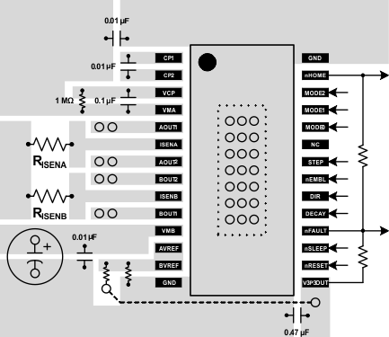 Figure 12. DRV8824-Q1 Board Layout