SLVSCH0 April 2014 DRV8824-Q1
PRODUCTION DATA.
- 1 Features
- 2 Applications
- 3 Description
- 4 Simplified Schematic
- 5 Revision History
- 6 Terminal Configuration and Functions
- 7 Specifications
- 8 Detailed Description
- 9 Application and Implementation
- 10Power Supply Recommendations
- 11Layout
- 12Device and Documentation Support
- 13Mechanical, Packaging, and Orderable Information
パッケージ・オプション
メカニカル・データ(パッケージ|ピン)
- PWP|28
サーマルパッド・メカニカル・データ
- PWP|28
発注情報
7 Specifications
7.1 Absolute Maximum Ratings
over operating free-air temperature range (unless otherwise noted) (1)(2)| VALUE | UNIT | |||
|---|---|---|---|---|
| VMx | Power supply voltage range | –0.3 to 47 | V | |
| Digital terminal voltage range | –0.5 to 7 | V | ||
| VREF | Input voltage | –0.3 to 4 | V | |
| ISENSEx terminal voltage | –0.3 to 0.8 | V | ||
| Peak motor drive output current, t < 1 μS | Internally limited | A | ||
| Continuous motor drive output current(3) | 1.6 | A | ||
| Continuous total power dissipation | See Thermal Information table | |||
| TJ | Operating virtual junction temperature range | –40 to 150 | °C | |
(1) Stresses beyond those listed under absolute maximum ratings may cause permanent damage to the device. These are stress ratings only, and functional operation of the device at these or any other conditions beyond those indicated under recommended operating conditions is not implied. Exposure to absolute maximum rated conditions for extended periods may affect device reliability.
(2) All voltage values are with respect to network ground terminal.
(3) Power dissipation and thermal limits must be observed.
7.2 Handling Ratings
| MIN | MAX | UNIT | ||
|---|---|---|---|---|
| Tstg | Storage temperature range | –60 | 150 | °C |
| VESD | HBD (human body model), AEC-Q100 Classification H2 | 2000 | V | |
| CDM (charged device model), AEC-Q100 Classification C4B | 750 |
7.3 Recommended Operating Conditions
| MIN | NOM | MAX | UNIT | ||
|---|---|---|---|---|---|
| VM | Motor power supply voltage(1) | 8.2 | 45 | V | |
| VREF | VREF input voltage(2) | 1 | 3.5 | V | |
| IV3P3 | V3P3OUT load current | 1 | mA | ||
(1) All VM terminals must be connected to the same supply voltage.
(2) Operational at VREF between 0 V and 1 V, but accuracy is degraded.
7.4 Thermal Information
| THERMAL METRIC | DRV8824-Q1 | UNIT | |
|---|---|---|---|
| PWP | |||
| 28 TERMINAL | |||
| RθJA | Junction-to-ambient thermal resistance(1) | 38.9 | °C/W |
| RθJC(top) | Junction-to-case (top) thermal resistance(2) | 23.3 | |
| RθJB | Junction-to-board thermal resistance(3) | 21.2 | |
| ψJT | Junction-to-top characterization parameter(4) | 0.8 | |
| ψJB | Junction-to-board characterization parameter(5) | 20.9 | |
| RθJC(bot) | Junction-to-case (bottom) thermal resistance(6) | 2.6 | |
(1) The junction-to-ambient thermal resistance under natural convection is obtained in a simulation on a JEDEC-standard, high-K board, as specified in JESD51-7, in an environment described in JESD51-2a.
(2) The junction-to-case (top) thermal resistance is obtained by simulating a cold plate test on the package top. No specific JEDEC-standard test exists, but a close description can be found in the ANSI SEMI standard G30-88.
(3) The junction-to-board thermal resistance is obtained by simulating in an environment with a ring cold plate fixture to control the PCB temperature, as described in JESD51-8.
(4) The junction-to-top characterization parameter, ψJT, estimates the junction temperature of a device in a real system and is extracted from the simulation data for obtaining θJA, using a procedure described in JESD51-2a (sections 6 and 7).
(5) The junction-to-board characterization parameter, ψJB, estimates the junction temperature of a device in a real system and is extracted from the simulation data for obtaining θJA , using a procedure described in JESD51-2a (sections 6 and 7).
(6) The junction-to-case (bottom) thermal resistance is obtained by simulating a cold plate test on the exposed (power) pad. No specific JEDEC standard test exists, but a close description can be found in the ANSI SEMI standard G30-88.
7.5 Electrical Characteristics
over operating free-air temperature range of -40°C to 125°C (unless otherwise noted)7.6 Timing Requirements
| MIN | MAX | UNIT | |||
|---|---|---|---|---|---|
| 1 | fSTEP | Step frequency | 250 | kHz | |
| 2 | tWH(STEP) | Pulse duration, STEP high | 1.9 | μs | |
| 3 | tWL(STEP) | Pulse duration, STEP low | 1.9 | μs | |
| 4 | tSU(STEP) | Setup time, command to STEP rising | 200 | ns | |
| 5 | tH(STEP) | Hold time, command to STEP rising | 200 | ns | |
| 6 | tENBL | Enable time, nENBL active to STEP | 200 | ns | |
| 7 | tWAKE | Wakeup time, nSLEEP inactive to STEP | 1 | ms | |
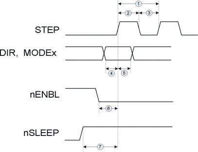 Figure 1. Timing Diagram
7.7 Typical Characteristics