JAJSSV1B December 2017 – January 2024 FPC202
PRODUCTION DATA
- 1
- 1 特長
- 2 アプリケーション
- 3 概要
- 4 Device Comparison Table
- 5 Pin Configuration and Functions
- 6 Specifications
-
7 Detailed Description
- 7.1 Overview
- 7.2 Functional Block Diagram
- 7.3
Feature Description
- 7.3.1 Host-Side Control Interface
- 7.3.2 LED Control
- 7.3.3 Low-Speed Output Signal Control
- 7.3.4 Low-Speed Input Status and Interrupt Generation
- 7.3.5 Downstream (Port-Side) I2C Master
- 7.3.6 Data Pre-Fetch From Modules
- 7.3.7 Scheduled Write
- 7.3.8 Protocol Timeouts
- 7.3.9 General-Purpose Inputs/Outputs
- 7.3.10 Hot-Plug Support
- 7.4 Device Functional Modes
- 7.5 Programming
- 8 Application and Implementation
- 9 Device and Documentation Support
- 10Revision History
- 11Mechanical, Packaging, and Orderable Information
7.3.2.1 Configurations with up to eight LEDs per port
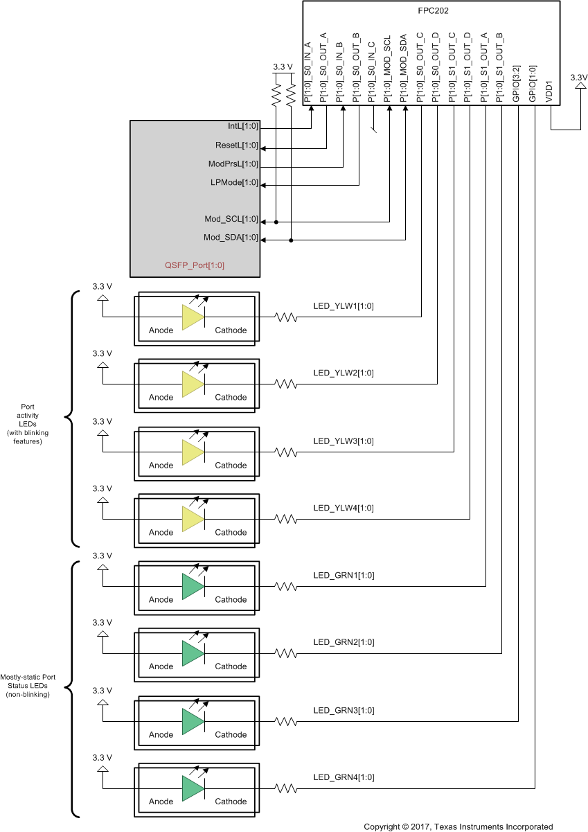
In some applications it may be desirable to control more than four LEDs per port. In cases where the additional LEDs are relatively static in nature and blinking is not required, the FPC202’s GPIO and unused OUT_* pins (for example, S1_OUT_A and S1_OUT_B) can be allocated for driving these LEDs in an active-low configuration. S0_OUT_C, S0_OUT_D, S1_OUT_C, and S1_OUT_D should be connected to LEDs requiring blinking and/or dimming, and up to four additional LEDs can be controlled per port from the GPIO, S1_OUT_A, and S1_OUT_B pins. Figure 7-2 shows an example of how up to eight LEDs can be controlled per port.
 Figure 7-2 Example Configuration for Driving Eight LEDs Per Port